ZHCSAD1D October 2012 – June 2017 TPD5S115
PRODUCTION DATA.
- 1 特性
- 2 应用
- 3 说明
- 4 修订历史记录
- 5 Pin Configuration and Functions
-
6 Specifications
- 6.1 Absolute Maximum Ratings
- 6.2 ESD Ratings
- 6.3 Recommended Operating Conditions
- 6.4 Thermal Information
- 6.5 Electrical Characteristics
- 6.6 Electrical Characteristics - I/O Capacitances
- 6.7 Switching Characteristics - VCCA = 1.2 V
- 6.8 Switching Characteristics - VCCA = 1.5 V
- 6.9 Switching Characteristics - VCCA = 1.8 V
- 6.10 Switching Characteristics - VCCA = 2.5 V
- 6.11 Switching Characteristics - VCCA = 3.3 V
- 6.12 Typical Characteristics
- 7 Detailed Description
- 8 Application and Implementation
- 9 Power Supply Recommendations
- 10Layout
- 11器件和文档支持
- 12机械、封装和可订购信息
8 Application and Implementation
NOTE
Information in the following applications sections is not part of the TI component specification, and TI does not warrant its accuracy or completeness. TI’s customers are responsible for determining suitability of components for their purposes. Customers should validate and test their design implementation to confirm system functionality.
8.1 Application Information
The TPD5S115 is an integrated solution for HDMI 2.0, 1.3, and 1.4 interfaces. The device has a boost converter on the power supply, signal conditioning circuits on CEC, SCL, SDA, and HPD lines, and ESD protection on all the connector-facing lines.
8.2 Typical Applications
8.2.1 DDC or CEC Level Shifter
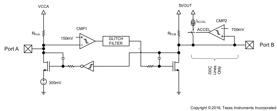
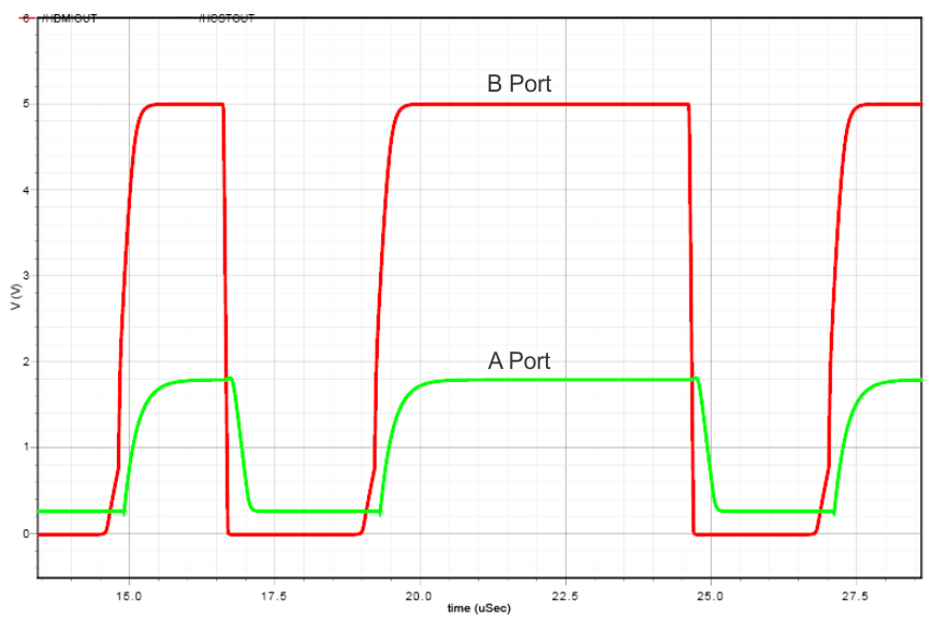
The TPD5S115 enables DDC translation from VCCA (system side) voltage levels to 5-V (HDMI cable side) voltage levels without degradation of system performance. The TPD5S115 contains 2 bidirectional, open-drain buffers specifically designed to support up and down-translation between the low voltage, VCCA side DDC-bus and the 5-V DDC-bus. The port B I/Os are overvoltage tolerant to 5.5 V, even when the device is shutdown. After power up and with the LS_OE and EN pins HIGH, a LOW level on port A (below VILC = 0.08 × VCCA) turns the corresponding port B driver (either SDA or SCL) on and drives port B down to VOLB. When port A rises above approximately 0.10 × VCCA, the port B pulldown driver is turned off and the internal pullup resistor pulls the pin HIGH. When port B falls first and goes below 0.3 × VOUT, a CMOS hysteresis input buffer detects the falling edge, turns on the port A driver, and pulls port A down to approximately VOLA = 0.16 × VCCA. The port B pulldown is not enabled unless the port A voltage goes below VILC. If the port A low voltage goes below VILC, the port B pulldown driver is enabled until port A rises above (VILC + ΔVT-HYSTA), then port B, if not externally driven LOW, continues to rise being pulled up by the internal pullup resistor.
 Figure 13. DDC or CEC Level Shifter Block Diagram
8.2.1.1 Design Requirements
For this design example, use the parameters listed in Table 1 as the input parameters.
Table 1. Design Parameters
| PARAMETER | VALUE |
|---|---|
| 5VOUT DC current | 55 mA |
| CEC_A, HPD_A, SCL_A, SDA_A voltage level | VCCA |
| HDMI 2.0 data rate per TMDS signal pair | 6 Gbps |
| Required IEC 61000-4-2 ESD Protection | ±8-kV contact |
8.2.1.2 Detailed Design Procedure
8.2.1.2.1 DDC or CEC Level Shifter Operational Notes for VCCA = 1.8 V
- The threshold of CMP1 is approximately 150 mV ± the 40 mV of total hysteresis
- The comparator trips for a falling waveform at approximately 130 mV
- The comparator trips for a rising waveform at approximately 170 mV
- To be recognized as a zero, the level at port A must first go below 130 mV (VILC in spec) and then stay below 170 mV (VILA in spec)
- To be recognized as a one, the level at A must first go above 170 mV and then stay above 130 mV
- VILC is specified as 110 mV in Electrical Characteristics to give some margin to the 130 mV
- VILA is specified as 140 mV in Electrical Characteristics to give some margin to the 170 mV
- VIHA is specified as 70% of VCCA to be consistent with standard CMOS levels
8.2.1.2.2 Input Capacitor
Due to the nature of the boost converter having a pulsating input current, a low-ESR input capacitor is required to prevent large voltage transients that can cause poor performance of the device or interference with other circuits in the system. TI recommends a 1.2-µF (minimum) input capacitor to improve transient behavior of the regulator and EMI behavior of the total power-supply circuit. TI recommends placing a ceramic capacitor (4.7 µF) as close as possible to the VIN and GND pins to improve the input noise filtering.
8.2.1.2.3 Output Capacitor
TI recommends using a small ceramic capacitors placed as close as possible to the VOUT and GND pins of the IC. If the application requires the use of large capacitors which can not be placed close to the IC, TI recommends using a smaller ceramic capacitor in parallel to the large capacitor. This small capacitor must be placed as close as possible to the VOUT and GND pins of the IC. Use Equation 1 to estimate the recommended minimum output capacitance.

where
- f is the switching frequency
- ΔV is the maximum allowed ripple
If a ripple voltage of 10 mV is chosen, a minimum effective capacitance of 2.7 µF is needed. The total ripple is larger due to the ESR of the output capacitor. This additional component of the ripple can be calculated using Equation 2.

To maintain control loop stability, a capacitor with a value in the range of the calculated minimum must be used. There are no additional requirements regarding minimum ESR. There is no upper limit for the output capacitance value. Larger capacitors cause lower output voltage ripple as well as lower output voltage drop during load transients.
Ceramic capacitors have a DC-bias effect, which has a strong influence on the final effective capacitance needed. Therefore the appropriate capacitor value must be chosen very carefully. Package size, voltage rating, and material are responsible for differences between the rated capacitor value and the effective capacitance. The minimum effective capacitance value is 1.2 µF, but the recommended value is 4.7 µF.
8.2.1.3 Application Curve
 Figure 14. DDC Level Shifter Operation (B to A Direction)
8.2.2 Other Application Circuits
Figure 15 and Figure 16 show application examples using the TPD5S115 devices. Customers must fully validate and test any circuit before implementing a design based on an example in this section. Unless otherwise noted, the design procedures in DDC or CEC Level Shifter are applicable.
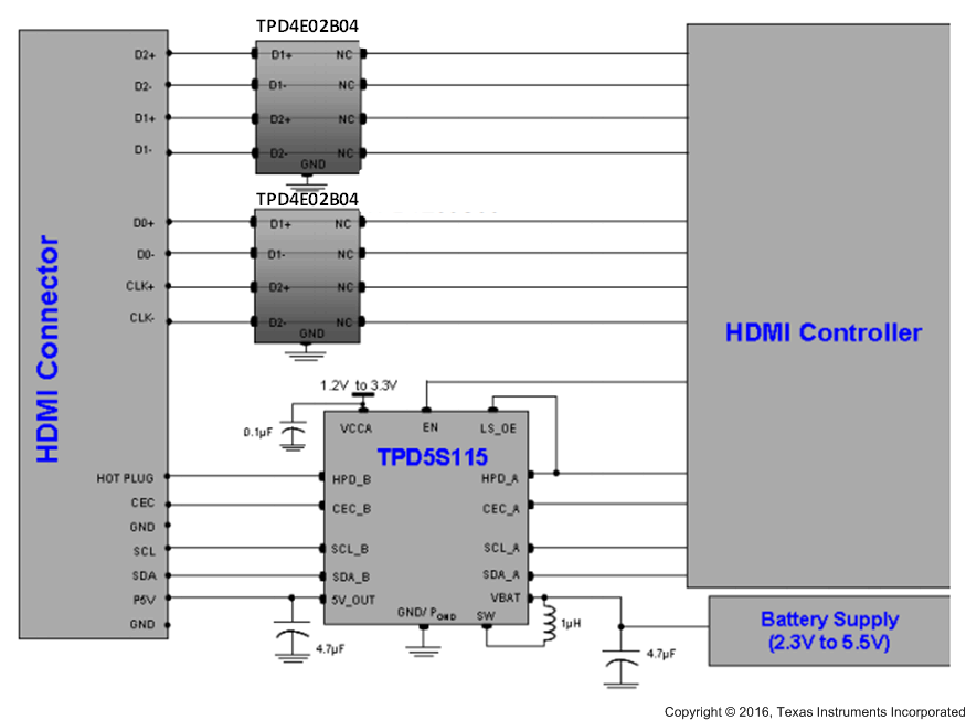
 Figure 15. Application Schematic for HDMI Controllers With One GPIO for HDMI Interface Control
Some HDMI controllers may have only one GPIO to control the HDMI interface, thus, the HDMI driver chip controls the TPD5S115 through only one control line (EN). In this mode the HPD_A to LS_OE pins are connected to each other (see Figure 15).
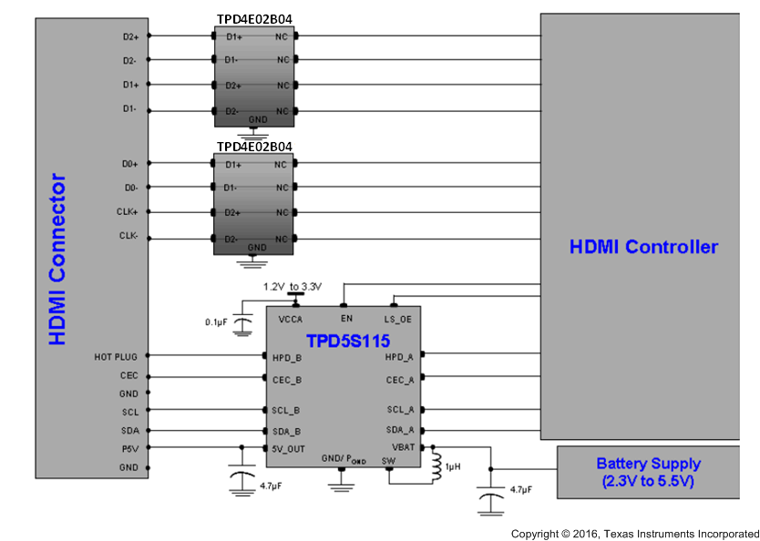
 Figure 16. Application Schematic for HDMI Controllers With Two GPIOs for HDMI Interface Control
Some HDMI driver chips may have two GPIOs to control the HDMI interface chip. In this case a flexible power saving mode can be implemented. The LS_OE and EN are active-high enable pins. They control the TPD5S115 power-saving options according to Table 3 and Table 4.
Table 3. Device Status – Part 1
| LS_OE | EN | VCCA | VBAT | 5VOUT | A-SIDE PULLUPS | DCC, B-SIDE PULLUPS | CEC, B-SIDE PULLUPS |
|---|---|---|---|---|---|---|---|
| L | L | 1.8 V | 5 V | Off | Off | Off | Off |
| L | H | 1.8 V | 5 V | On | On | On | Off |
| H | L | 1.8 V | 5 V | Off | Off | Off | Off |
| H | H | 1.8 V | 5 V | On | On | On | On |
| X | X | 0 V | 0 V | High-Z | High-Z | High-Z | High-Z |
| X | X | 1.8 V | 0 V | Low | Low | High-Z | High-Z |
| X | X | 0 V | 5 V | High-Z | High-Z | High-Z | High-Z |
Table 4. Device Status – Part 2
| LS_OE | EN | CEC LDO | DC-DC AND HPD | DDC OR CEC VLTS | ICCA TYP | ICC VBAT TYP | COMMENT |
|---|---|---|---|---|---|---|---|
| L | L | Off | Off | OFF and High-Z | 1 µA | 1 µA | Fully disabled |
| L | H | Off | On | OFF and High-Z | 1 µA | 30 µA | DC-DC (30 µA) ON |
| H | L | Off | Off | OFF and High-Z | 1 µA | 1 µA | Not valid state |
| H | H | On | On | ON | 13 µA | 225 µA | Fully ON |
| X | X | Off | Off | High-Z | 0 µA | 0 µA | Power down |
| X | X | Off | Off | High-Z | 0 µA | 0 µA | Power down |
| X | X | Off | Off | High-Z | 0 µA | 0 µA | Power down |