ZHCSDL8A December   2014  – February 2015 TPD6F002-Q1

PRODUCTION DATA.  

  1. 特性
  2. 应用
  3. 说明
  4. 简化电路原理图
  5. 修订历史记录
  6. Pin Configuration and Functions
  7. Specifications
    1. 7.1 Absolute Maximum Ratings
    2. 7.2 ESD Ratings
    3. 7.3 Recommended Operating Conditions
    4. 7.4 Thermal Information
    5. 7.5 Electrical Characteristics
    6. 7.6 Typical Characteristics
  8. Detailed Description
    1. 8.1 Overview
    2. 8.2 Functional Block Diagram
    3. 8.3 Feature Description
      1. 8.3.1 AEC-Q101 Qualified
      2. 8.3.2 Six-Channel EMI Filtering
      3. 8.3.3 Pi-Style Filter Configuration
      4. 8.3.4 Robust ESD Protection
      5. 8.3.5 Low Leakage Current
      6. 8.3.6 Space-Saving SON Package
    4. 8.4 Device Functional Modes
  9. Application and Implementation
    1. 9.1 Application Information
    2. 9.2 Typical Application
      1. 9.2.1 Design Requirements
      2. 9.2.2 Detailed Design Procedure
        1. 9.2.2.1 Signal Range on All Protected Lines
        2. 9.2.2.2 Operating Frequency
        3. 9.2.2.3 Crosstalk Response
      3. 9.2.3 Application Curves
  10. 10Power Supply Recommendations
  11. 11Layout
    1. 11.1 Layout Guidelines
    2. 11.2 Layout Example
  12. 12器件和文档支持
    1. 12.1 商标
    2. 12.2 静电放电警告
    3. 12.3 术语表
  13. 13机械、封装和可订购信息

封装选项

机械数据 (封装 | 引脚)
散热焊盘机械数据 (封装 | 引脚)
订购信息

6 Pin Configuration and Functions

DSV PACKAGE
(3.0 mm × 1.35 mm × 0.75 mm)
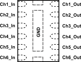
TPD6F002-Q1 po_lls876.gif

Pin Functions

PIN I/O DESCRIPTION
NAME NO.
ChX_In 1, 2, 3, 4, 5, 6 IO ESD-protected channel, connected to corresponding ChX_Out
ChX_Out 7, 8, 9, 10, 11, 12 IO ESD-protected channel, connected to corresponding ChX_In
GND G G Ground