ZHCSDL8A December 2014 – February 2015 TPD6F002-Q1
PRODUCTION DATA.
8 Detailed Description
8.1 Overview
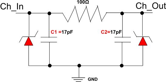
The TPD6F002-Q1 is a highly integrated device that provides a six channel EMI filter and a TVS based ESD protection diode array. The low-pass filter array suppresses EMI/RFI emissions for data ports subject to electromagnetic interference. The TPD6F002-Q1 is rated to dissipate ESD strikes above the maximum level specified in the IEC 61000-4-2 international standard. The high level of integration, combined with its small easy-to-route DSV package, makes this device ideal for protecting interfaces like LCD displays, memory interfaces, and FPD-Link.
8.2 Functional Block Diagram

8.3 Feature Description
The TPD6F002-Q1 is a highly integrated device that provides a six channel EMI filter and a TVS based ESD protection diode array. The low-pass filter array suppresses EMI/RFI emissions for data ports subject to electromagnetic interference. The TVS diode array is rated to dissipate ESD strikes above the maximum level specified in the IEC 61000-4-2 international standard. The high level of integration, combined with its small easy-to-route DSV package, allows this device to provide great circuit protection for LCD displays, memory interfaces, GPIO lines, and FPD-Link.
8.3.1 AEC-Q101 Qualified
This device is qualified to AEC-Q101 standards. It passes HBM H3B (±8 kV) and CDM C5 (±1 kV) ESD ratings and is qualified to operate from –40°C to 125°C.
8.3.2 Six-Channel EMI Filtering
This device provides six channels for EMI filtering of data lines with the following parameters:
- –47 dB Crosstalk Attenuation at 100 MHz
- –30 dB Insertion Loss at 800 MHz
- –3 dB Bandwidth: 100 MHz
8.3.3 Pi-Style Filter Configuration
This device has a pi-style filtering configuration composed of a series resistor and two capacitors in parallel with the I/O pins. The typical resistor value is 100 Ω and the typical capacitor values are 17 pF each.
8.3.4 Robust ESD Protection
The ESD protection on all pins exceeds the IEC 61000-4-2 level 4 standard. Contact ESD is rated at ±20 kV and Air-gap ESD is rated at ±30 kV.
8.3.5 Low Leakage Current
The I/O pins feature an ultra-low leakage current of 20-nA (max) with a bias of 3.3 V
8.3.6 Space-Saving SON Package
The layout of this device makes it easy to add protection to existing layouts. The packages offer flow-through routing which requires minimal changes to existing layout for addition of these devices. Additionally, the device offers a small space-saving package that takes a minimal footprint on the board.
8.4 Device Functional Modes
The TPD6F002-Q1 is a passive integrated circuit that passively filters EMI and triggers when voltages are above VBR or below the lower diode voltage (–0.6 V). During ESD events, voltages as high as ±30 kV (air) can be directed to ground via the internal diode network. Once the voltages on the protected line fall below the trigger levels, the device reverts to passive.