SLLS876B August 2008 – May 2016 TPD6F002
PRODUCTION DATA.
- 1 Features
- 2 Applications
- 3 Description
- 4 Revision History
- 5 Pin Configuration and Functions
- 6 Specifications
- 7 Detailed Description
- 8 Application and Implementation
- 9 Power Supply Recommendations
- 10Layout
- 11Device and Documentation Support
- 12Mechanical, Packaging, and Orderable Information
封装选项
请参考 PDF 数据表获取器件具体的封装图。
机械数据 (封装 | 引脚)
- DSV|12
散热焊盘机械数据 (封装 | 引脚)
- DSV|12
订购信息
8 Application and Implementation
NOTE
Information in the following applications sections is not part of the TI component specification, and TI does not warrant its accuracy or completeness. TI’s customers are responsible for determining suitability of components for their purposes. Customers should validate and test their design implementation to confirm system functionality.
8.1 Application Information
The TPD6F002 offers highly-integrated ESD protection and EMI filtering for 6 channels per device. Take care during implementation to make sure that this device fits the application appropriately.
8.2 Typical Application
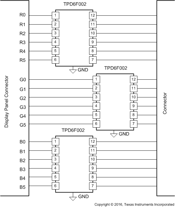
 Figure 5. Display Panel Schematic
8.2.1 Design Requirements
For this design example, three TPD6F002 devices are being used in an 18-bit display panel application. This provides a complete ESD and EMI protection solution for the display connector.
Table 1 lists the parameters for this display panel application.
Table 1. Design Parameters
| DESIGN PARAMETER | VALUE |
|---|---|
| Signal range on all pins except GND | 0 V to 5 V |
| Operating Frequency | 50 MHz |
8.2.2 Detailed Design Procedure
To begin the design process, some design parameters must be decided; the designer must know the following:
- Signal range of all the protected lines
- Operating frequency
- Crosstalk response
8.2.2.1 Signal Range on All Protected Lines
The TPD6F002 has 6 identical protection channels for signal lines. All I/O pins support a signal range from 0 to 5.5 V.
8.2.2.2 Operating Frequency
The TPD6F002 has a 100-MHz, –3-dB bandwidth, which supports the operating frequency for this display.
8.2.2.3 Crosstalk Response
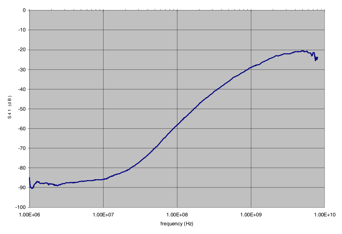
The TPD6F002 has a –57-dB crosstalk attenuation at 100 MHz, sufficient for this display.
8.2.3 Application Curve
 Figure 6. Channel-to-Channel Crosstalk