SLLS876B August 2008 – May 2016 TPD6F002
PRODUCTION DATA.
- 1 Features
- 2 Applications
- 3 Description
- 4 Revision History
- 5 Pin Configuration and Functions
- 6 Specifications
- 7 Detailed Description
- 8 Application and Implementation
- 9 Power Supply Recommendations
- 10Layout
- 11Device and Documentation Support
- 12Mechanical, Packaging, and Orderable Information
封装选项
请参考 PDF 数据表获取器件具体的封装图。
机械数据 (封装 | 引脚)
- DSV|12
散热焊盘机械数据 (封装 | 引脚)
- DSV|12
订购信息
6 Specifications
6.1 Absolute Maximum Ratings
over operating free-air temperature range (unless otherwise noted)(1)| MIN | MAX | UNIT | |||
|---|---|---|---|---|---|
| VIO | I/O to GND | 6 | V | ||
| Lead temperature (soldering, 10 s) | 300 | °C | |||
| TJ | Junction temperature | 150 | °C | ||
| Tstg | Storage temperature | –65 | 150 | °C | |
(1) Stresses beyond those listed under Absolute Maximum Ratings may cause permanent damage to the device. These are stress ratings only, which do not imply functional operation of the device at these or any other conditions beyond those indicated under Recommended Operating Conditions. Exposure to absolute-maximum-rated conditions for extended periods may affect device reliability.
6.2 ESD Ratings
| VALUE | UNIT | |||
|---|---|---|---|---|
| V(ESD) | Electrostatic discharge | Human-body model(1) | ±15000 | V |
| IEC 61000-4-2 contact discharge | ±20000 | |||
| IEC 61000-4-2 air-gap discharge | ±30000 | |||
(1) JEDEC document JEP155 states that 500-V HBM allows safe manufacturing with a standard ESD control process.
6.3 Recommended Operating Conditions
over operating free-air temperature range (unless otherwise noted)| MIN | MAX | UNIT | ||
|---|---|---|---|---|
| VIO | Input pin voltage | 0 | 5.5 | V |
| TA | Operating free-air temperature | –40 | 85 | °C |
6.4 Thermal Information
| THERMAL METRIC(1) | TPD6F002 | UNIT | |
|---|---|---|---|
| DSV (WSON) | |||
| 12 PINS | |||
| RθJA | Junction-to-ambient thermal resistance | 120.7 | °C/W |
| RθJC(top) | Junction-to-case (top) thermal resistance | 104.4 | °C/W |
| RθJB | Junction-to-board thermal resistance | 78.5 | °C/W |
| ψJT | Junction-to-top characterization parameter | 13 | °C/W |
| ψJB | Junction-to-board characterization parameter | 77.7 | °C/W |
| RθJC(bot) | Junction-to-case (bottom) thermal resistance | 66.5 | °C/W |
(1) For more information about traditional and new thermal metrics, see the Semiconductor and IC Package Thermal Metrics application report, SPRA953.
6.5 Electrical Characteristics
TA = –40°C to 85°C (Unless otherwise noted)| PARAMETER | TEST CONDITIONS | MIN | TYP(1) | MAX | UNIT | |
|---|---|---|---|---|---|---|
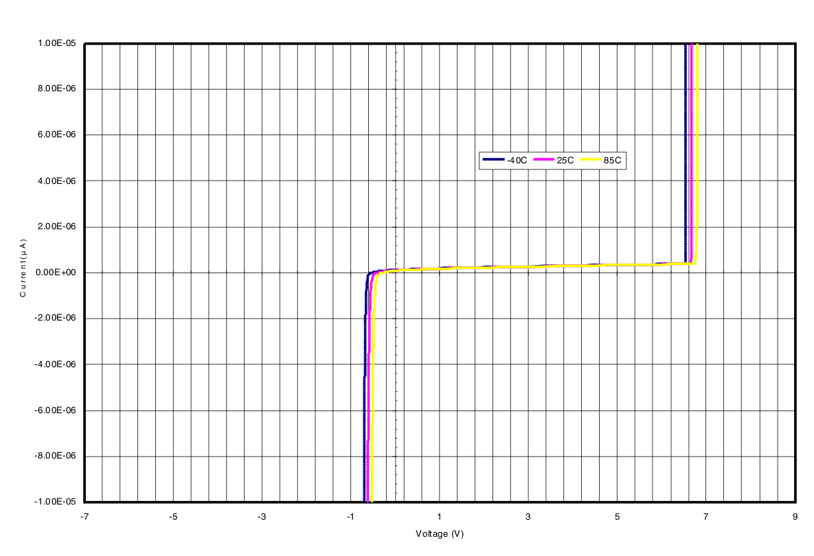
| VBR | DC breakdown voltage | IIO = 10 μA | 6 | V | ||
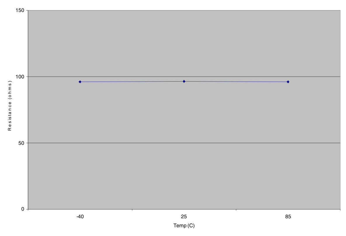
| R | Resistance | 85 | 100 | 115 | Ω | |
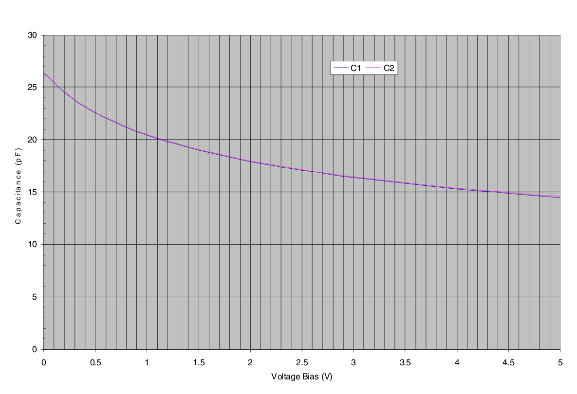
| C | Capacitance (C1 or C2) | VIO = 2.5 V | 17 | pF | ||
| IIO | Channel leakage current | VIO = 3.3 V | 1 | 20 | nA | |
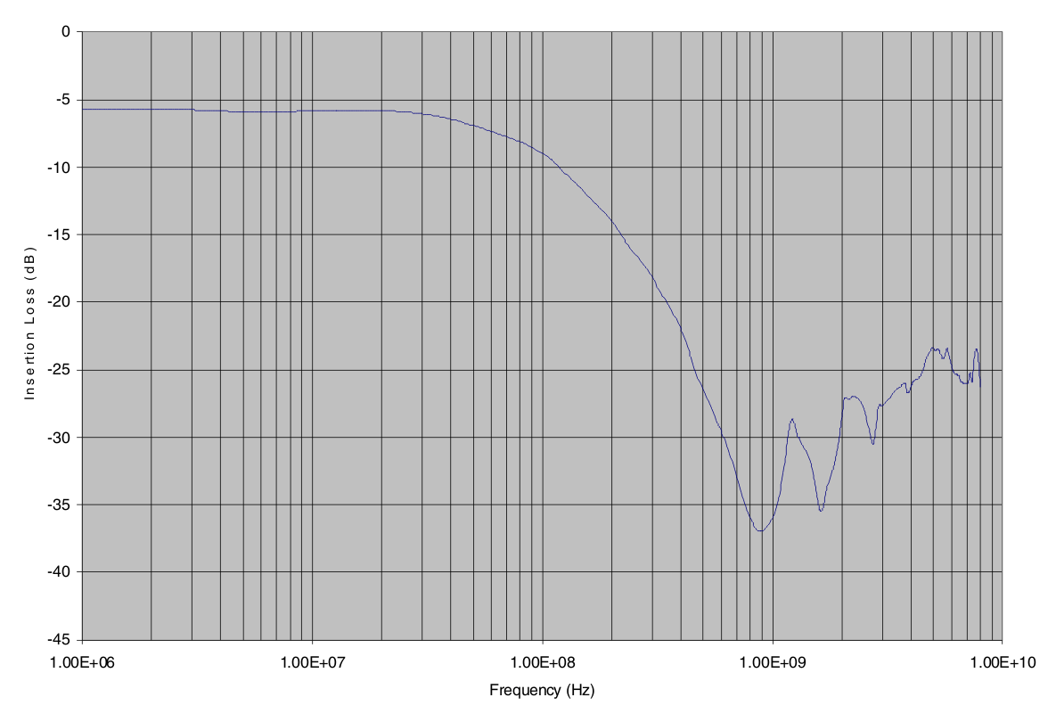
| fC | Cutoff frequency | ZSOURCE = 50 Ω, ZLOAD = 50 Ω | 100 | MHz | ||
(1) Typical values are at TA = 25°C.
6.6 Typical Characteristics
 Figure 1. DC Voltage-Current Sweep Across Input, Output Pins

| TA = 25°C, DC Bias = 0 V, 50 Ω Environment |
 Figure 2. Series Resistance vs Temperature
