ZHCSG02C September 2016 – January 2017 TPD6S300
PRODUCTION DATA.
- 1 特性
- 2 应用
- 3 说明
- 4 修订历史记录
- 5 Device Comparison Table
- 6 Pin Configuration and Functions
- 7 Specifications
-
8 Detailed Description
- 8.1 Overview
- 8.2 Functional Block Diagram
- 8.3
Feature Description
- 8.3.1 4-Channels of Short-to-VBUS Overvoltage Protection (CC1, CC2, SBU1, SBU2 Pins): 24-VDC Tolerant
- 8.3.2 8-Channels of IEC 61000-4-2 ESD Protection (CC1, CC2, SBU1, SBU2, DP_T, DM_T, DP_B, DM_B Pins)
- 8.3.3 CC1, CC2 Overvoltage Protection FETs 600 mA Capable for Passing VCONN Power
- 8.3.4 CC Dead Battery Resistors Integrated for Handling the Dead Battery Use Case in Mobile Devices
- 8.3.5 3-mm × 3-mm WQFN Package
- 8.4 Device Functional Modes
- 9 Application and Implementation
- 10Power Supply Recommendations
- 11Layout
- 12器件和文档支持
- 13机械、封装和可订购信息
7 Specifications
7.1 Absolute Maximum Ratings
over operating free-air temperature range (unless otherwise noted)(1)| MIN | MAX | UNIT | |||
|---|---|---|---|---|---|
| VI | Input voltage | VPWR | –0.3 | 5 | V |
| RPD_G1, RPD_G2 | –0.3 | 24 | V | ||
| VO | Output voltage | FLT | –0.3 | 6 | V |
| VBIAS | –0.3 | 24 | V | ||
| VIO | I/O voltage | D1, D2 | –0.3 | 6 | V |
| CC1, CC2, SBU1, SBU2 | –0.3 | 6 | V | ||
| C_CC1, C_CC2, C_SBU1, C_SBU2 | –0.3 | 24 | V | ||
| TA | Operating free air temperature | –40 | 85 | °C | |
| Tstg | Storage temperature | –65 | 150 | °C | |
(1) Stresses beyond those listed under Absolute Maximum Ratings may cause permanent damage to the device. These are stress ratings only, which do not imply functional operation of the device at these or any other conditions beyond those indicated under Recommended Operating Conditions. Exposure to absolute-maximum-rated conditions for extended periods may affect device reliability.
7.2 ESD Ratings—JEDEC Specification
| VALUE | UNIT | ||||
|---|---|---|---|---|---|
| V(ESD) | Electrostatic discharge | Human-body model (HBM), per ANSI/ESDA/JEDEC JS-001(1) | ±2000 | V | |
| Charged-device model (CDM), per JEDEC specification JESD22-C101(2) | ±500 | ||||
(1) JEDEC document JEP155 states that 500-V HBM allows safe manufacturing with a standard ESD control process. Pins listed as ±2000 V may actually have higher performance.
(2) JEDEC document JEP157 states that 250-V CDM allows safe manufacturing with a standard ESD control process. Pins listed as ±500 V may actually have higher performance.
7.3 ESD Ratings—IEC Specification
| VALUE | UNIT | ||||
|---|---|---|---|---|---|
| V(ESD) | Electrostatic discharge(1) | IEC 61000-4-2, C_CC1, C_CC2, D1, D2 | Contact discharge | ±8000 | V |
| Air-gap discharge | ±15000 | ||||
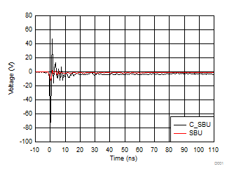
| IEC 61000-4-2, C_SBU1, C_SBU2 | Contact discharge | ±6000 | |||
| Air-gap discharge | ±15000 | ||||
7.4 Recommended Operating Conditions
over operating free-air temperature range (unless otherwise noted)| MIN | NOM | MAX | UNIT | |||
|---|---|---|---|---|---|---|
| VI | Input voltage | VPWR | 2.7 | 3.3 | 4.5 | V |
| RPD_G1, RPD_G2 | 0 | 5.5 | V | |||
| VO | Output voltage | FLT pull-up resistor power rail | 2.7 | 5.5 | V | |
| VIO | I/O voltage | D1, D2 | –0.3 | 5.5 | V | |
| CC1, CC2, C_CC1, C_CC2 | 0 | 5.5 | V | |||
| SBU1, SBU2, C_SBU1, C_SBU2 | 0 | 4.3 | V | |||
| IVCONN | VCONN current | Current flowing into CC1/2 and flowing out of C_CC1/2, VCCx – VC_CCx ≤ 250 mV | 600 | mA | ||
| IVCONN | VCONN current | Current flowing into CC1/2 and flowing out of C_CC1/2, TJ ≤ 105°C | 1.25 | A | ||
| External components(1) | FLT pull-up resistance | 1.7 | 300 | kΩ | ||
| VBIAS capacitance(2) | 0.1 | µF | ||||
| VPWR capacitance | 0.3 | 1 | µF | |||
(1) For recommended values for capacitors and resistors, the typical values assume a component placed on the board near the pin. Minimum and maximum values listed are inclusive of manufacturing tolerances, voltage derating, board capacitance, and temperature variation. The effective value presented must be within the minimum and maximums listed in the table.
(2) The VBIAS pin requires a minimum 35-VDC rated capacitor. A 50-VDC rated capacitor is recommended to reduce capacitance derating. See the VBIAS Capacitor Selection section for more information on selecting the VBIAS capacitor.
7.5 Thermal Information
| THERMAL METRIC(1) | TPD6S300 | UNIT | |
|---|---|---|---|
| RUK (WQFN) | |||
| 20 PINS | |||
| RθJA | Junction-to-ambient thermal resistance | 45.2 | °C/W |
| RθJC(top) | Junction-to-case (top) thermal resistance | 48.8 | °C/W |
| RθJB | Junction-to-board thermal resistance | 17.1 | °C/W |
| ψJT | Junction-to-top characterization parameter | 0.6 | °C/W |
| ψJB | Junction-to-board characterization parameter | 17.1 | °C/W |
| RθJC(bot) | Junction-to-case (bottom) thermal resistance | 3.7 | °C/W |
(1) For more information about traditional and new thermal metrics, see the Semiconductor and IC Package Thermal Metrics application report.
7.6 Electrical Characteristics
over operating free-air temperature range (unless otherwise noted)| PARAMETER | TEST CONDITIONS | MIN | TYP | MAX | UNIT | |
|---|---|---|---|---|---|---|
| CC OVP SWITCHES | ||||||
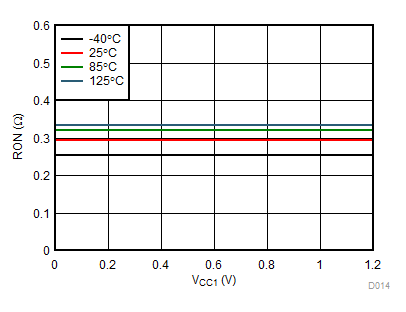
| RON | On resistance of CC OVP FETs, TJ ≤ 85°C | CCx = 5.5 V | 278 | 392 | mΩ | |
| On resistance of CC OVP FETs, TJ ≤ 105°C | CCx = 5.5 V | 278 | 415 | mΩ | ||
| RON(FLAT) | On resistance flatness | Sweep CCx voltage between 0 V and 1.2 V | 5 | mΩ | ||
| CON_CC | Equivalent on capacitance | Capacitance from C_CCx or CCx to GND when device is powered. VC_CCx/VCCx = 0 V to 1.2 V, f = 400 kHz | 60 | 74 | 120 | pF |
| RD | Dead battery pull-down resistance (only present when device is unpowered). Effective resistance of RD and FET in series | V_C_CCx = 2.6 V | 4.1 | 5.1 | 6.1 | kΩ |
| VTH_DB | Threshold voltage of the pulldown FET in series with RD during dead battery | I_CC = 80 µA | 0.5 | 0.9 | 1.2 | V |
| VOVPCC | OVP threshold on CC pins | Place 5.5 V on C_CCx. Step up C_CCx until the FLT pin is asserted | 5.75 | 6 | 6.2 | V |
| VOVPCC_HYS | Hysteresis on CC OVP | Place 6.5 V on C_CCx. Step down the voltage on C_CCx until the FLT pin is deasserted. Measure difference between rising and falling OVP threshold for C_CCx | 50 | mV | ||
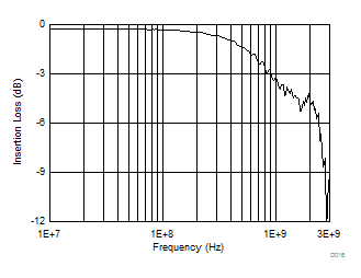
| BWON | On bandwidth single ended (–3 dB) | Measure the –3-dB bandwidth from C_CCx to CCx. Single ended measurement, 50-Ω system. Vcm = 0.1 V to 1.2 V | 100 | MHz | ||
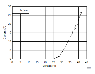
| VSTBUS_CC | Short-to-VBUS tolerance on the CC pins | Hot-Plug C_CCx with a 1 meter USB Type C Cable, place a 30-Ω load on CCx | 24 | V | ||
| VSTBUS_CC_CLAMP | Short-to-VBUS system-side clamping voltage on the CC pins (CCx) | Hot-Plug C_CCx with a 1 meter USB Type C Cable. Hot-Plug voltage C_CCx = 24 V. VPWR = 3.3 V. Place a 30-Ω load on CCx | 8 | V | ||
| SBU OVP SWITCHES | ||||||
| RON | On resistance of SBU OVP FETs | SBUx = 3.6 V. –40°C ≤ TJ ≤ +85°C | 4 | 6.5 | Ω | |
| RON(FLAT) | On resistance flatness | Sweep SBUx voltage between 0 V and 3.6 V. –40°C ≤ TJ ≤ +85°C | 0.7 | 1.5 | Ω | |
| CON_SBU | Equivalent on capacitance | Capacitance from SBUx or C_SBUx to GND when device is powered. Measure at VC_SBUx/VSBUx = 0.3 V to 3.6 V | 6 | pF | ||
| VOVPSBU | OVP threshold on SBU pins | Place 3.6 V on C_SBUx. Step up C_SBUx until the FLT pin is asserted | 4.35 | 4.5 | 4.7 | V |
| VOVPSBU_HYS | Hysteresis on SBU OVP | Place 5 V on C_CCx. Step down the voltage on C_CCx until the FLT pin is deasserted. Measure difference between rising and falling OVP threshold for C_SBUx | 50 | mV | ||
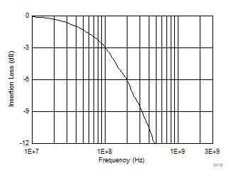
| BWON | On bandwidth single ended (–3 dB) | Measure the –3-dB bandwidth from C_SBUx to SBUx. Single ended measurement, 50-Ω system. Vcm = 0.1 V to 3.6 V | 1000 | MHz | ||
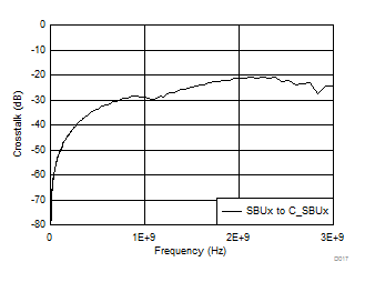
| XTALK | Crosstalk | Measure crosstalk at f = 1 MHz from SBU1 to C_SBU2 or SBU2 to C_SBU1. Vcm1 = 3.6 V, Vcm2 = 0.3 V. Be sure to terminate open sides to 50 Ω | –80 | dB | ||
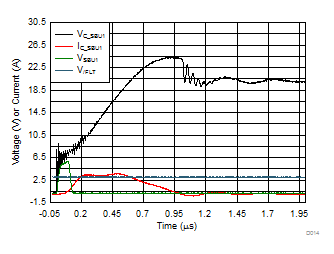
| VSTBUS_SBU | Short-to-VBUS tolerance on the SBU pins | Hot-Plug C_SBUx with a 1 meter USB Type C Cable. Put a 100-nF capacitor in series with a 40-Ω resistor to GND on SBUx | 24 | V | ||
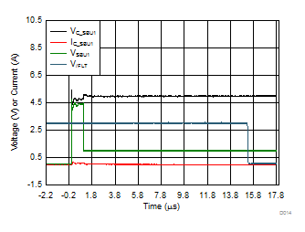
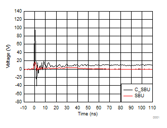
| VSTBUS_SBU_CLAMP | Short-to-VBUS system-side clamping voltage on the SBU pins (SBUx) | Hot-Plug C_SBUx with a 1 meter USB Type C Cable. Hot-Plug voltage C_SBUx = 24 V. VPWR = 3.3 V. Put a 150-nF capacitor in series with a 40-Ω resistor to GND on SBUx | 8 | V | ||
| POWER SUPPLY and LEAKAGE CURRENTS | ||||||
| VPWR_UVLO | VPWR under voltage lockout | Place 1 V on VPWR and raise voltage until SBU or CC FETs turnon | 2.1 | 2.3 | 2.5 | V |
| VPWR_UVLO_HYS | VPWR UVLO hysteresis | Place 3 V on VPWR and lower voltage until SBU or CC FETs turnoff; measure difference between rising and falling UVLO to calculate hysteresis | 100 | 150 | 200 | mV |
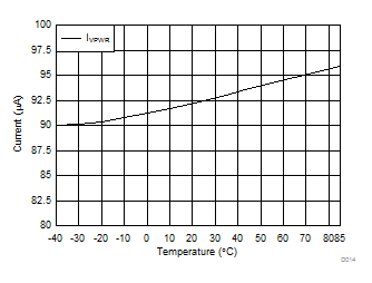
| IVPWR | VPWR supply current | VPWR = 3.3 V (typical), VPWR = 4.5 V (maximum). –40°C ≤ TJ ≤ +85°C. | 90 | 135 | µA | |
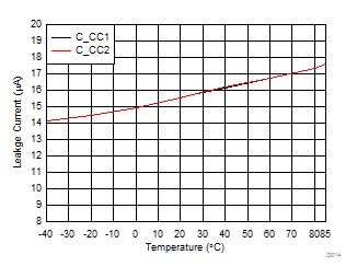
| ICC_LEAK | Leakage current for CC pins when device is powered | VPWR = 3.3 V, VC_CCx = 3.6 V, CCx pins are floating, measure leakage into C_CCx pins. Result must be same if CCx side is biased and C_CCx is left floating | 5 | µA | ||
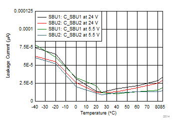
| ISBU_LEAK | Leakage current for SBU pins when device is powered | VPWR = 3.3 V, VC_SBUx = 3.6 V, SBUx pins are floating, measure leakge into C_SBUx pins. Result must be same if SBUx side is biased and C_SBUx is left floating. –40°C ≤ TJ ≤ +85°C | 3 | µA | ||
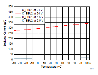
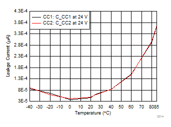
| IC_CC_LEAK_OVP | Leakage current for CC pins when device is in OVP | VPWR = 0 V or 3.3 V, VC_CCx = 24 V, CCx pins are set to 0 V, measure leakage into C_CCx pins | 1200 | µA | ||
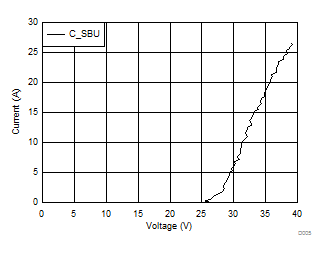
| IC_SBU_LEAK_OVP | Leakage current for SBU pins when device is in OVP | VPWR = 0 V or 3.3 V, VC_SBUx = 24 V, SBUx pins are set to 0 V, measure leakage into C_SBUx pins | 400 | µA | ||
| ICC_LEAK_OVP | Leakage current for CC pins when device is in OVP | VPWR = 0 V or 3.3 V, VC_CCx = 24 V, CCx pins are set to 0 V, measure leakage out of CCx pins | 30 | µA | ||
| ISBU_LEAK_OVP | Leakage current for SBU pins when device is in OVP | VPWR = 0 V or 3.3 V, VC_SBUx = 24 V, SBUx pins are set to 0 V, measure leakage out of SBUx pins | –1 | 1 | µA | |
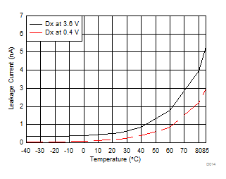
| IDx_LEAK | Leakage current for Dx pins | V_Dx = 3.6 V, measure leakage into Dx pins | 1 | µA | ||
| FLT PIN | ||||||
| VOL | Low-level output voltage | IOL = 3 mA. Measure the voltage at the FLT pin | 0.4 | V | ||
| OVER TEMPERATURE PROTECTION | ||||||
| TSD_RISING | The rising over-temperature protection shutdown threshold | 150 | 175 | °C | ||
| TSD_FALLING | The falling over-temperature protection shutdown threshold | 130 | 140 | °C | ||
| TSD_HYST | The over-temperature protection shutdown threshold hysteresis | 35 | °C | |||
| Dx ESD PROTECTION | ||||||
| VRWM_POS | Reverse stand-off voltage from Dx to GND | Dx to GND. IDX ≤ 1 µA | 5.5 | V | ||
| VRWM_NEG | Reverse stand-off voltage from GND to Dx | GND to Dx | 0 | V | ||
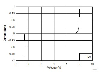
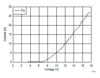
| VBR_POS | Break-down voltage from Dx to GND | Dx to GND. IBR = 1 mA | 7 | V | ||
| VBR_NEG | Break-down voltage from GND to Dx | GND to Dx. IBR = 8 mA | 0.6 | V | ||
| CIO | Dx to GND or GND to Dx | f = 1 MHz, VIO = 2.5 V | 1.7 | pF | ||
| ΔCIO | Differential capacitance between two Dx pins | f = 1 MHz, VIO = 2.5 V | 0.02 | pF | ||
| RDYN | Dynamic on-resistance Dx IEC clamps | Dx to GND or GND to Dx | 0.4 | Ω | ||
7.7 Timing Requirements
7.8 Typical Characteristics
