SLLSE33E August 2010 – December 2016 TPD7S019
PRODUCTION DATA.
8 Application and Implementation
NOTE
Information in the following applications sections is not part of the TI component specification, and TI does not warrant its accuracy or completeness. TI’s customers are responsible for determining suitability of components for their purposes. Customers should validate and test their design implementation to confirm system functionality.
8.1 Application Information
When a system contains a human interface connector, it becomes vulnerable to large system-level ESD strikes that standard ICs cannot survive. The TPD7S019 provides IEC61000-4-2 Level 4 Contact ESD rating to the VGA or DVI-I port. The integrated voltage level-shifting, buffering and termination reduce the board space needed to implement the control lines functions.
8.2 Typical Application
8.2.1 Design Requirements
In this application, the TPD7S019 is used to protect the VGA port. Table 1 lists the system parameters.
Table 1. Design Parameters
| DESIGN PARAMETER | VALUE |
|---|---|
| Pull-up resistors on DDC lines | 1.5 kΩ to 2 kΩ |
| Termination resistors on VIDEO lines | 50 Ω to 75 Ω |
| VIDEO signals data rate | 24 MHz to 388 MHz |
| Required IEC 61000-4-2 ESD Protection | ±8-kV Contact |
8.2.2 Detailed Design Procedure
To begin the design process, some parameters must be decided upon; the designer must make sure:
- Voltage range on the protected line must not exceed the reverse standoff voltage of the TVS diode(s) (VRWM)
- Operating frequency is supported by the I/O capacitance CIO of the TVS diode
- IEC 61000-4-2 protection requirement is covered by the IEC performance of the TVS diode
For this application, the DDC signals switch between 0 V and 5 V (with resistor pulling it up to 5-V power supply). The VIDEO and SYNC signal levels are between 0 V and VCC_VIDEO / VCC_SYNC. All signals are not exceeding the recommended values and the ESD cells on these pins stay untriggered.
Depending on the resolution and the refresh rate of the display, the VIDEO (RGB) signals' bandwidth can be from 24 MHz to 388 MHz. The line capacitances from the ESD cells are 2.5 pF typical which is only takes up a small portion of the total capacitance budget for the maximum frequency in this range.
±8-kV Contact ESD provided by the TPD7S019 meets the ESD design goal of ±8 kV contact.
Put 1.5-kΩ to 2-kΩ pullup resistor on the DDC lines to be compliant with the I2C standard. Termination resistors on VIDEO lines are 50 Ω to 75 Ω to match the impedance on board trace.
8.2.3 Application Curves
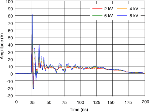
 Figure 7. IEC 61000-4-2 Clamping Voltage, Positive Contact
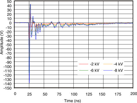
 Figure 8. IEC 61000-4-2 Clamping Voltage, Negative Contact
.gif)