SLLSE38B June 2010 – March 2016 TPD8E003
PRODUCTION DATA.
- 1 Features
- 2 Applications
- 3 Description
- 4 Revision History
- 5 Pin Configuration and Functions
- 6 Specifications
- 7 Detailed Description
- 8 Application and Implementation
- 9 Power Supply Recommendations
- 10Layout
- 11Device and Documentation Support
- 12Mechanical, Packaging, and Orderable Information
8 Application and Implementation
NOTE
Information in the following applications sections is not part of the TI component specification, and TI does not warrant its accuracy or completeness. TI’s customers are responsible for determining suitability of components for their purposes. Customers should validate and test their design implementation to confirm system functionality.
8.1 Application Information
The TPD8E003 offers eight ESD clamp circuits in a space-saving DQD package. When placed near the connector, the TPD8E003 ESD solution offers little or no signal distortion during normal operation due to low IO capacitance and ultra-low leakage current specifications. The TPD8E003 ensures that the core circuitry is protected and the system is functioning properly in the event of an ESD strike.
8.2 Typical Application
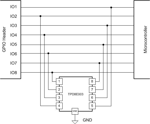
 Figure 4. GPIO Header Application
8.2.1 Design Requirements
For this design example, one TPD8E003 is used to protect an 8-pin GPIO header.
Given the example application, the parameters listed in Table 1 are known.
Table 1. Design Parameters
| PARAMETER | VALUE |
|---|---|
| Signal Range on Protected Lines | 0 V to 5 V |
| Required Level of IEC ESD Protection | ±8kV Contact, ±15kV Air Gap |
8.2.2 Detailed Design Procedure
To begin the design process, some parameters must be decided upon; the designer must know the following:
- Voltage range of the signal on all protected lines
- Required ESD protection needed
8.2.2.1 Signal Range
The TPD8E003 supports signal ranges between 0 V and 5.5 V, which supports the GPIO application.
8.2.2.2 Required ESD Protection
The TPD8E003 is rated to withstand up to ±12-kV contact and ±15-kV air gap IEC ESD. This meets the IEC ESD design target with room to spare.
8.2.3 Application Curves
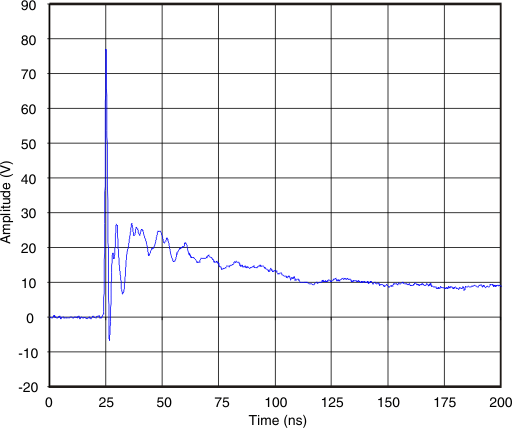
 Figure 5. IEC ESD Clamping Waveforms
8-kV Contact
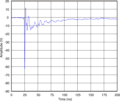
 Figure 6. IEC ESD Clamping Waveforms
–8-kV Contact