SLLSE38B June 2010 – March 2016 TPD8E003
PRODUCTION DATA.
- 1 Features
- 2 Applications
- 3 Description
- 4 Revision History
- 5 Pin Configuration and Functions
- 6 Specifications
- 7 Detailed Description
- 8 Application and Implementation
- 9 Power Supply Recommendations
- 10Layout
- 11Device and Documentation Support
- 12Mechanical, Packaging, and Orderable Information
10 Layout
10.1 Layout Guidelines
For proper operation of the ESD clamps, both during normal function and ESD events, the following layout and design guidelines must be followed:
- Place the TPD8E003 solution close to the connector. This allows the TPD8E003 to take away the energy associated with ESD strike before it reaches the internal circuitry of the system board.
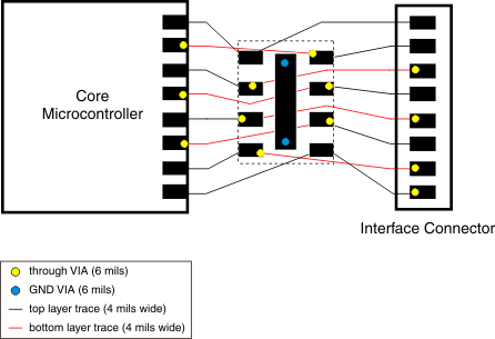
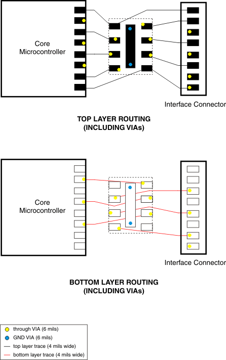
- TI recommends employing two signal layers in the printed-circuit board (PCB) to route through the eight ESD clamp terminals of the TPD8E003.
- Ensure that there is proper metallization for the GND vertical interconnect access (VIA). During an ESD event, the in-rush current flows to the system GND plane through the GND VIA. Having a low-impedance path allows the current to flow quickly to GND, effectively building a robust, system-level ESD immunity.
- Place the VIA under the DQD pad in locations that offer maximum flexibility in board routing.
- One common set of guidelines (not restricted to all cases):
- Trace width: 4 mm
- VIA diameter: 6 mm
- DQD package pad dimensions: 8 mm × 12 mm
10.2 Layout Example
 Figure 7. Board Layout With the TPD8E003DQDR
 Figure 8. Top and Bottom Layer Board Layout With the TPD8E003DQDR