ZHCSG00B September 2016 – November 2016 TPD8S300
PRODUCTION DATA.
- 1 特性
- 2 应用
- 3 说明
- 4 修订历史记录
- 5 Device Comparison Table
- 6 Pin Configuration and Functions
- 7 Specifications
-
8 Detailed Description
- 8.1 Overview
- 8.2 Functional Block Diagram
- 8.3
Feature Description
- 8.3.1 4-Channels of Short-to-VBUS Overvoltage Protection (CC1, CC2, SBU1, SBU2 Pins): 24-VDC Tolerant
- 8.3.2 8-Channels of IEC 61000-4-2 ESD Protection (CC1, CC2, SBU1, SBU2, DP_T, DM_T, DP_B, DM_B Pins)
- 8.3.3 CC1, CC2 Overvoltage Protection FETs 600 mA Capable for Passing VCONN Power
- 8.3.4 CC Dead Battery Resistors Integrated for Handling the Dead Battery Use Case in Mobile Devices
- 8.3.5 3-mm × 3-mm WQFN Package
- 8.4 Device Functional Modes
- 9 Application and Implementation
- 10Power Supply Recommendations
- 11Layout
- 12器件和文档支持
- 13机械、封装和可订购信息
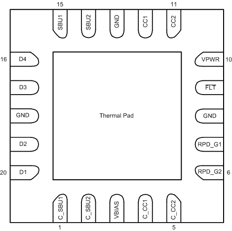
6 Pin Configuration and Functions
RUK Package
20 Pin WQFN
Top View

Pin Functions
| PIN | TYPE | DESCRIPTION | |
|---|---|---|---|
| NO. | NAME | ||
| 1 | C_SBU1 | I/O | Connector side of the SBU1 OVP FET. Connect to either SBU pin of the USB Type-C connector |
| 2 | C_SBU2 | I/O | Connector side of the SBU2 OVP FET. Connect to either SBU pin of the USB Type-C connector |
| 3 | VBIAS | Power | Pin for ESD support capacitor. Place a 0.1-µF capacitor on this pin to ground |
| 4 | C_CC1 | I/O | Connector side of the CC1 OVP FET. Connect to either CC pin of the USB Type-C connector |
| 5 | C_CC2 | I/O | Connector side of the CC2 OVP FET. Connect to either CC pin of the USB Type-C connector |
| 6 | RPD_G2 | I/O | Short to C_CC2 if dead battery resistors are needed. If dead battery resistors are not needed, short pin to GND |
| 7 | RPD_G1 | I/O | Short to C_CC1 if dead battery resistors are needed. If dead battery resistors are not needed, short pin to GND |
| 8 | GND | GND | Ground |
| 9 | FLT | O | Open drain for fault reporting |
| 10 | VPWR | Power | 2.7-V-3.6-V power supply |
| 11 | CC2 | I/O | System side of the CC2 OVP FET. Connect to either CC pin of the CC/PD controller |
| 12 | CC1 | I/O | System side of the CC1 OVP FET. Connect to either CC pin of the CC/PD controller |
| 13 | GND | GND | Ground |
| 14 | SBU2 | I/O | System side of the SBU2 OVP FET. Connect to either SBU pin of the SBU MUX |
| 15 | SBU1 | I/O | System side of the SBU1 OVP FET. Connect to either SBU pin of the SBU MUX |
| 16 | D4 | I/O | USB2.0 IEC ESD protection. Connect to any of the USB2.0 pins of the USB Type-C connector |
| 17 | D3 | I/O | USB2.0 IEC ESD protection. Connect to any of the USB2.0 pins of the USB Type-C connector |
| 18 | GND | GND | Ground |
| 19 | D2 | I/O | USB2.0 IEC ESD protection. Connect to any of the USB2.0 pins of the USB Type-C connector |
| 20 | D1 | I/O | USB2.0 IEC ESD protection. Connect to any of the USB2.0 pins of the USB Type-C connector |
| — | Thermal Pad | GND | Internally connected to GND. Used as a heatsink. Connect to the PCB GND plane |