ZHCSE79C March 2011 – September 2015
PRODUCTION DATA.
- 1 特性
- 2 应用
- 3 说明
- 4 修订历史记录
- 5 Pin Configuration and Functions
- 6 Specifications
-
7 Detailed Description
- 7.1 Overview
- 7.2 Functional Block Diagram
- 7.3 Feature Description
- 7.4 Device Functional Modes
- 7.5 Programming with I2C
- 7.6
Register Maps
- 7.6.1 Slave Address
- 7.6.2 TPL0102 Register Map
- 7.6.3 IVRA (Initial Value Register for Potentiometer A)
- 7.6.4 WRA (Wiper Resistance Register for Potentiometer A)
- 7.6.5 IVRB (Initial Value Register for Potentiometer B)
- 7.6.6 WRB (Wiper Resistance Register for Potentiometer B)
- 7.6.7 ACR (Access Control Register)
- 8 Application and Implementation
- 9 Power Supply Recommendations
- 10Layout
- 11器件和文档支持
- 12机械、封装和可订购信息
封装选项
机械数据 (封装 | 引脚)
散热焊盘机械数据 (封装 | 引脚)
- RUC|14
订购信息
10 Layout
10.1 Layout Guidelines
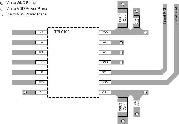
To ensure reliability of the device, please follow common printed-circuit board layout guidelines.
- Leads to the input should be as direct as possible with a minimum conductor length.
- The ground path should have low resistance and low inductance.
- Short trace-lengths should be used to avoid excessive loading.
- It is common to have a dedicated ground plane on an inner layer of the board.
- Terminals that are connected to ground should have a low-impedance path to the ground plane in the form of wide polygon pours and multiple vias.
- Bypass capacitors should be used on power supplies and should be placed as close as possible to the VDD and VSS pins.
- Apply low equivalent series resistance 0.1 µF to 10 µF tantalum or electrolytic capacitors at the supplies to minimize transient disturbances and to filter low frequency ripple.
- To reduce the total I2C bus capacitance added by PCB parasitics, data lines (SCL and SDA) should be a short as possible and the widths of the traces should also be minimized (e.g. 5-10 mils depending on copper weight).
10.2 Layout Example
 Figure 37. TPL0102 Layout Example