ZHCSE79C March 2011 – September 2015
PRODUCTION DATA.
- 1 特性
- 2 应用
- 3 说明
- 4 修订历史记录
- 5 Pin Configuration and Functions
- 6 Specifications
-
7 Detailed Description
- 7.1 Overview
- 7.2 Functional Block Diagram
- 7.3 Feature Description
- 7.4 Device Functional Modes
- 7.5 Programming with I2C
- 7.6
Register Maps
- 7.6.1 Slave Address
- 7.6.2 TPL0102 Register Map
- 7.6.3 IVRA (Initial Value Register for Potentiometer A)
- 7.6.4 WRA (Wiper Resistance Register for Potentiometer A)
- 7.6.5 IVRB (Initial Value Register for Potentiometer B)
- 7.6.6 WRB (Wiper Resistance Register for Potentiometer B)
- 7.6.7 ACR (Access Control Register)
- 8 Application and Implementation
- 9 Power Supply Recommendations
- 10Layout
- 11器件和文档支持
- 12机械、封装和可订购信息
封装选项
机械数据 (封装 | 引脚)
散热焊盘机械数据 (封装 | 引脚)
- RUC|14
订购信息
7 Detailed Description
7.1 Overview
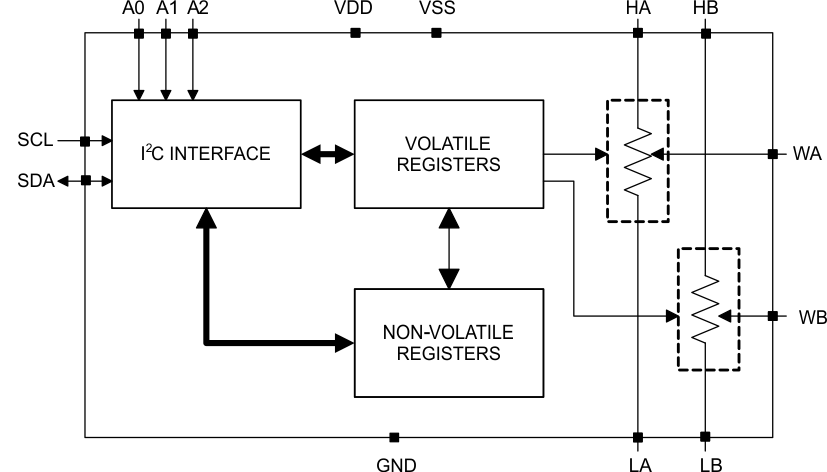
The TPL0102 has two linear-taper digital potentiometers with 256 wiper positions and an end-to-end resistance of 100 kΩ. Each potentiometer can be used as a three-terminal potentiometer or as a two-terminal rheostat. The two potentiometers can both be used in Voltage Divider Mode, Rheostat Mode, or Shutdown Mode at the same time, or any combination of those modes. For example, potentiometer A can be used in Voltage Divider Mode and potentiometer B can be used in Voltage Divider Mode, or potentiometer A can be used in Voltage Divider Mode and potentiometer B can be used in Rheostat Mode. The two potentiometers are functionally independent of one another.
The High (H) and Low (L) terminals of the TPL0102 are equivalent to the fixed terminals of a mechanical potentiometer. The H and L terminals do not have any polarity restrictions (H can be at a higher voltage than L, or L can be at a higher voltage than H). The position of the wiper (W) terminal is controlled by the value in the Wiper Resistance (WR) 8-bit register. When the WR register contains all zeroes (zero-scale), the wiper terminal is closest to its L terminal. As the value of the WR register increases from all zeroes to all ones (full-scale), the wiper moves monotonically from the position closest to L terminal to the position closest to the H terminal. At the same time, the resistance between W and L increases monotonically, whereas the resistance between W and H decreases monotonically.
The TPL0102 has non-volatile memory (EEPROM) which can be used to store the wiper position. When the device is powered down, the last value stored in the Initial Value Register (IVR) will be maintained in the non-volatile memory. When power is restored, the contents of the IVR are automatically recalled and loaded into the corresponding WR register to set the wipers . The internal registers of the TPL0102 can be accessed using the I2C interface. The factory-programmed default value for the IVR upon power up is 0x80h (1000 0000). The WR register can be written to directly without first writing to the IVR, depending upon the setting of the volatile memory (VOL) in the ACR (Access Control Register). If the WR register is written to directly without writing to the IVR as well, this results in the wiper position changing to a desired position, but the position will not be stored in memory and will not be reloaded upon powering up the device.
With one TPL0102, a variable resistor with 512 settings can be used since there are two potentiometers in one TPL0102. In order to achieve this, the two potentiometers should be in Rheostat Mode and wired so that terminal L of potentiometer B is tied to terminal W of potentiometer A. This will provide 512 settings between terminal L of potentiometer A and terminal W of potentiometer B.
7.2 Functional Block Diagram
7.3 Feature Description
The TPL0102 has two linear-taper digital potentiometers (DPOTs) with 256 wiper positions. Each potentiometer can be used as a three-terminal potentiometer or a two-terminal rheostat. The TPL0102-100 has an end-to-end resistance of 100 kΩ with a 20% end-to-end resistance tolerance. Non-volatile memory (EEPROM) can be used to store the wiper position allowing the wiper position to be stored even during power-off and automatically reinstated after power-on. The internal registers of the TPL0102 can be accessed using the I2C digital interface. The TPL0102 is available in a 14-pin MicroQFN (2.00 mm x 2.00 mm) and 14-pin TSSOP package.
7.4 Device Functional Modes
7.4.1 Shutdown Mode
The TPL0102 can be put in Shutdown Mode by executing the proper command in the ACR (Access Control Register). Please see the TPL0102 Register Map for more details. When active, this feature causes terminal H to become high impedance.
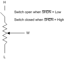 Figure 18. Equivalent Circuit for Shutdown Mode
7.4.2 Voltage Divider Mode
The digital potentiometer generates a voltage divider when all three terminals are used. The voltage divider at wiper-to-H and wiper-to-L is proportional to the input voltage at H to L.
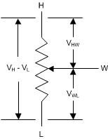 Figure 19. Equivalent Circuit for Voltage Divider Mode
For example, connecting terminal H to 5 V and terminal L to ground, the output voltage at terminal W can range from 0 V to 5 V. The general equation defining the output voltage at terminal W for any valid input voltage applied to terminal H and terminal L is

The voltage difference between terminal H and terminal W can also be calculated

where
- D is the decimal value of the wiper code.
7.4.3 Rheostat Mode
The TPL0102 operates in rheostat mode when only two terminals are used as a variable resistor. The variable resistance can either be between terminal H and terminal W or between terminal L and terminal W. The unused terminal can be left floating or it can be tied to terminal W. The nominal resistance between terminal H and terminal L is 100 kΩ and has 256 tap points accessed by the wiper terminal. The 8-bit volatile register value is used to determine one of the 256 possible wiper positions.
In rheostat mode, to set the resistance between terminal H and terminal W, the potentiometer can be configured in two possible ways.
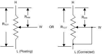 Figure 20. Equivalent Circuit for Rheostat Mode with Terminal H to Terminal W Resistance
The general equation for determining the digitally programmed output resistance between Terminal H and Terminal W is:

where
- RTOT is the end-to-end resistance between terminal H and terminal L.
- D is the decimal value of the wiper code.
Similarly, to set the resistance between terminal L and terminal W, the potentiometer can be configured in two possible ways.
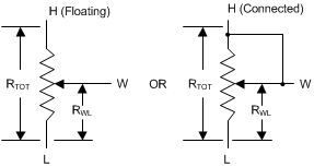 Figure 21. Equivalent Circuit for Rheostat Mode with Terminal L to Terminal W Resistance
The general equation for determining the digitally programmed output resistance between terminal L and terminal W is

where
- RTOT is the end-to-end resistance between terminal H and terminal L.
- D is the decimal value of the wiper code.
The following table shows the ideal values for DPOT with End-to End resistance of 100 kΩ. The absolute values of resistance can vary significantly but the Ratio (RWL/RHW) is extremely accurate.
The linearity values are "relative" linearity values (i.e. linearity after zero-scale and full-scale offset errors are removed). Please take this into account when expecting a certain absolute accuracy since some error will be introduced once you get close in magnitude to the offset errors.
| Step | Hex | Binary | RWL (kΩ) | RHW (kΩ) | RWL/RHW |
|---|---|---|---|---|---|
| 0 (zero-scale) | 0x00h | 0000 0000 | 0.00 | 100.00 | 0.00 |
| 1 | 0x01h | 0000 0001 | 0.39 | 99.61 | 0.00 |
| 2 | 0x02h | 0000 0010 | 0.78 | 99.22 | 0.01 |
| 3 | 0x03h | 0000 0011 | 1.17 | 98.83 | 0.01 |
| 4 | 0x04h | 0000 0100 | 1.56 | 98.44 | 0.02 |
| 5 | 0x05h | 0000 0101 | 1.95 | 98.05 | 0.02 |
| 6 | 0x06h | 0000 0110 | 2.34 | 97.66 | 0.02 |
| 7 | 0x07h | 0000 0111 | 2.73 | 97.27 | 0.03 |
| 8 | 0x08h | 0000 1000 | 3.13 | 96.88 | 0.03 |
| 9 | 0x09h | 0000 1001 | 3.52 | 96.48 | 0.04 |
| 10 | 0x0Ah | 0000 1010 | 3.91 | 96.09 | 0.04 |
| 11 | 0x0Bh | 0000 1011 | 4.30 | 95.70 | 0.04 |
| 12 | 0x0Ch | 0000 1100 | 4.69 | 95.31 | 0.05 |
| 13 | 0x0Dh | 0000 1101 | 5.08 | 94.92 | 0.05 |
| 14 | 0x0Eh | 0000 1110 | 5.47 | 94.53 | 0.06 |
| 15 | 0x0Fh | 0000 1111 | 5.86 | 94.14 | 0.06 |
| 16 | 0x10h | 0001 0000 | 6.25 | 93.75 | 0.07 |
| 17 | 0x11h | 0001 0001 | 6.64 | 93.36 | 0.07 |
| 18 | 0x12h | 0001 0010 | 7.03 | 92.97 | 0.08 |
| 19 | 0x13h | 0001 0011 | 7.42 | 92.58 | 0.08 |
| 20 | 0x14h | 0001 0100 | 7.81 | 92.19 | 0.08 |
| 21 | 0x15h | 0001 0101 | 8.20 | 91.80 | 0.09 |
| 22 | 0x16h | 0001 0110 | 8.59 | 91.41 | 0.09 |
| 23 | 0x17h | 0001 0111 | 8.98 | 91.02 | 0.10 |
| 24 | 0x18h | 0001 1000 | 9.38 | 90.63 | 0.10 |
| 25 | 0x19h | 0001 1001 | 9.77 | 90.23 | 0.11 |
| 26 | 0x1Ah | 0001 1010 | 10.16 | 89.84 | 0.11 |
| 27 | 0x1Bh | 0001 1011 | 10.55 | 89.45 | 0.12 |
| 28 | 0x1Ch | 0001 1100 | 10.94 | 89.06 | 0.12 |
| 29 | 0x1Dh | 0001 1101 | 11.33 | 88.67 | 0.13 |
| 30 | 0x1Eh | 0001 1110 | 11.72 | 88.28 | 0.13 |
| 31 | 0x1Fh | 0001 1111 | 12.11 | 87.89 | 0.14 |
| 32 | 0x20h | 0010 0000 | 12.50 | 87.50 | 0.14 |
| 33 | 0x21h | 0010 0001 | 12.89 | 87.11 | 0.15 |
| 34 | 0x22h | 0010 0010 | 13.28 | 86.72 | 0.15 |
| 35 | 0x23h | 0010 0011 | 13.67 | 86.33 | 0.16 |
| 36 | 0x24h | 0010 0100 | 14.06 | 85.94 | 0.16 |
| 37 | 0x25h | 0010 0101 | 14.45 | 85.55 | 0.17 |
| 38 | 0x26h | 0010 0110 | 14.84 | 85.16 | 0.17 |
| 39 | 0x27h | 0010 0111 | 15.23 | 84.77 | 0.18 |
| 40 | 0x28h | 0010 1000 | 15.63 | 84.38 | 0.19 |
| 41 | 0x29h | 0010 1001 | 16.02 | 83.98 | 0.19 |
| 42 | 0x2Ah | 0010 1010 | 16.41 | 83.59 | 0.20 |
| 43 | 0x2Bh | 0010 1011 | 16.80 | 83.20 | 0.20 |
| 44 | 0x2Ch | 0010 1100 | 17.19 | 82.81 | 0.21 |
| 45 | 0x2Dh | 0010 1101 | 17.58 | 82.42 | 0.21 |
| 46 | 0x2Eh | 0010 1110 | 17.97 | 82.03 | 0.22 |
| 47 | 0x2Fh | 0010 1111 | 18.36 | 81.64 | 0.22 |
| 48 | 0x30h | 0011 0000 | 18.75 | 81.25 | 0.23 |
| 49 | 0x31h | 0011 0001 | 19.14 | 80.86 | 0.24 |
| 50 | 0x32h | 0011 0010 | 19.53 | 80.47 | 0.24 |
| 51 | 0x33h | 0011 0011 | 19.92 | 80.08 | 0.25 |
| 52 | 0x34h | 0011 0100 | 20.31 | 79.69 | 0.25 |
| 53 | 0x35h | 0011 0101 | 20.70 | 79.30 | 0.26 |
| 54 | 0x36h | 0011 0110 | 21.09 | 78.91 | 0.27 |
| 55 | 0x37h | 0011 0111 | 21.48 | 78.52 | 0.27 |
| 56 | 0x38h | 0011 1000 | 21.88 | 78.13 | 0.28 |
| 57 | 0x39h | 0011 1001 | 22.27 | 77.73 | 0.29 |
| 58 | 0x3Ah | 0011 1010 | 22.66 | 77.34 | 0.29 |
| 59 | 0x3Bh | 0011 1011 | 23.05 | 76.95 | 0.30 |
| 60 | 0x3Ch | 0011 1100 | 23.44 | 76.56 | 0.31 |
| 61 | 0x3Dh | 0011 1101 | 23.83 | 76.17 | 0.31 |
| 62 | 0x3Eh | 0011 1110 | 24.22 | 75.78 | 0.32 |
| 63 | 0x3Fh | 0011 1111 | 24.61 | 75.39 | 0.33 |
| 64 | 0x40h | 0100 0000 | 25.00 | 75.00 | 0.33 |
| 65 | 0x41h | 0100 0001 | 25.39 | 74.61 | 0.34 |
| 66 | 0x42h | 0100 0010 | 25.78 | 74.22 | 0.35 |
| 67 | 0x43h | 0100 0011 | 26.17 | 73.83 | 0.35 |
| 68 | 0x44h | 0100 0100 | 26.56 | 73.44 | 0.36 |
| 69 | 0x45h | 0100 0101 | 26.95 | 73.05 | 0.37 |
| 70 | 0x46h | 0100 0110 | 27.34 | 72.66 | 0.38 |
| 71 | 0x47h | 0100 0111 | 27.73 | 72.27 | 0.38 |
| 72 | 0x48h | 0100 1000 | 28.13 | 71.88 | 0.39 |
| 73 | 0x49h | 0100 1001 | 28.52 | 71.48 | 0.40 |
| 74 | 0x4Ah | 0100 1010 | 28.91 | 71.09 | 0.41 |
| 75 | 0x4Bh | 0100 1011 | 29.30 | 70.70 | 0.41 |
| 76 | 0x4Ch | 0100 1100 | 29.69 | 70.31 | 0.42 |
| 77 | 0x4Dh | 0100 1101 | 30.08 | 69.92 | 0.43 |
| 78 | 0x4Eh | 0100 1110 | 30.47 | 69.53 | 0.44 |
| 79 | 0x4Fh | 0100 1111 | 30.86 | 69.14 | 0.45 |
| 80 | 0x50h | 0101 0000 | 31.25 | 68.75 | 0.45 |
| 81 | 0x51h | 0101 0001 | 31.64 | 68.36 | 0.46 |
| 82 | 0x52h | 0101 0010 | 32.03 | 67.97 | 0.47 |
| 83 | 0x53h | 0101 0011 | 32.42 | 67.58 | 0.48 |
| 84 | 0x54h | 0101 0100 | 32.81 | 67.19 | 0.49 |
| 85 | 0x55h | 0101 0101 | 33.20 | 66.80 | 0.50 |
| 86 | 0x56h | 0101 0110 | 33.59 | 66.41 | 0.51 |
| 87 | 0x57h | 0101 0111 | 33.98 | 66.02 | 0.51 |
| 88 | 0x58h | 0101 1000 | 34.38 | 65.63 | 0.52 |
| 89 | 0x59h | 0101 1001 | 34.77 | 65.23 | 0.53 |
| 90 | 0x5Ah | 0101 1010 | 35.16 | 64.84 | 0.54 |
| 91 | 0x5Bh | 0101 1011 | 35.55 | 64.45 | 0.55 |
| 92 | 0x5Ch | 0101 1100 | 35.94 | 64.06 | 0.56 |
| 93 | 0x5Dh | 0101 1101 | 36.33 | 63.67 | 0.57 |
| 94 | 0x5Eh | 0101 1110 | 36.72 | 63.28 | 0.58 |
| 95 | 0x5Fh | 0101 1111 | 37.11 | 62.89 | 0.59 |
| 96 | 0x60h | 0110 0000 | 37.50 | 62.50 | 0.60 |
| 97 | 0x61h | 0110 0001 | 37.89 | 62.11 | 0.61 |
| 98 | 0x62h | 0110 0010 | 38.28 | 61.72 | 0.62 |
| 99 | 0x63h | 0110 0011 | 38.67 | 61.33 | 0.63 |
| 100 | 0x64h | 0110 0100 | 39.06 | 60.94 | 0.64 |
| 101 | 0x65h | 0110 0101 | 39.45 | 60.55 | 0.65 |
| 102 | 0x66h | 0110 0110 | 39.84 | 60.16 | 0.66 |
| 103 | 0x67h | 0110 0111 | 40.23 | 59.77 | 0.67 |
| 104 | 0x68h | 0110 1000 | 40.63 | 59.38 | 0.68 |
| 105 | 0x69h | 0110 1001 | 41.02 | 58.98 | 0.70 |
| 106 | 0x6Ah | 0110 1010 | 41.41 | 58.59 | 0.71 |
| 107 | 0x6Bh | 0110 1011 | 41.80 | 58.20 | 0.72 |
| 108 | 0x6Ch | 0110 1100 | 42.19 | 57.81 | 0.73 |
| 109 | 0x6Dh | 0110 1101 | 42.58 | 57.42 | 0.74 |
| 110 | 0x6Eh | 0110 1110 | 42.97 | 57.03 | 0.75 |
| 111 | 0x6Fh | 0110 1111 | 43.36 | 56.64 | 0.77 |
| 112 | 0x70h | 0111 0000 | 43.75 | 56.25 | 0.78 |
| 113 | 0x71h | 0111 0001 | 44.14 | 55.86 | 0.79 |
| 114 | 0x72h | 0111 0010 | 44.53 | 55.47 | 0.80 |
| 115 | 0x73h | 0111 0011 | 44.92 | 55.08 | 0.82 |
| 116 | 0x74h | 0111 0100 | 45.31 | 54.69 | 0.83 |
| 117 | 0x75h | 0111 0101 | 45.70 | 54.30 | 0.84 |
| 118 | 0x76h | 0111 0110 | 46.09 | 53.91 | 0.86 |
| 119 | 0x77h | 0111 0111 | 46.48 | 53.52 | 0.87 |
| 120 | 0x78h | 0111 1000 | 46.88 | 53.13 | 0.88 |
| 121 | 0x79h | 0111 1001 | 47.27 | 52.73 | 0.90 |
| 122 | 0x7Ah | 0111 1010 | 47.66 | 52.34 | 0.91 |
| 123 | 0x7Bh | 0111 1011 | 48.05 | 51.95 | 0.92 |
| 124 | 0x7Ch | 0111 1100 | 48.44 | 51.56 | 0.94 |
| 125 | 0x7Dh | 0111 1101 | 48.83 | 51.17 | 0.95 |
| 126 | 0x7Eh | 0111 1110 | 49.22 | 50.78 | 0.97 |
| 127 | 0x7Fh | 0111 1111 | 49.61 | 50.39 | 0.98 |
| 128 | 0x80h | 1000 0000 | 50.00 | 50.00 | 1.00 |
| 129 | 0x81h | 1000 0001 | 50.39 | 49.61 | 1.02 |
| 130 | 0x82h | 1000 0010 | 50.78 | 49.22 | 1.03 |
| 131 | 0x83h | 1000 0011 | 51.17 | 48.83 | 1.05 |
| 132 | 0x84h | 1000 0100 | 51.56 | 48.44 | 1.06 |
| 133 | 0x85h | 1000 0101 | 51.95 | 48.05 | 1.08 |
| 134 | 0x86h | 1000 0110 | 52.34 | 47.66 | 1.10 |
| 135 | 0x87h | 1000 0111 | 52.73 | 47.27 | 1.12 |
| 136 | 0x88h | 1000 1000 | 53.13 | 46.88 | 1.13 |
| 137 | 0x89h | 1000 1001 | 53.52 | 46.48 | 1.15 |
| 138 | 0x8Ah | 1000 1010 | 53.91 | 46.09 | 1.17 |
| 139 | 0x8Bh | 1000 1011 | 54.30 | 45.70 | 1.19 |
| 140 | 0x8Ch | 1000 1100 | 54.69 | 45.31 | 1.21 |
| 141 | 0x8Dh | 1000 1101 | 55.08 | 44.92 | 1.23 |
| 142 | 0x8Eh | 1000 1110 | 55.47 | 44.53 | 1.25 |
| 143 | 0x8Fh | 1000 1111 | 55.86 | 44.14 | 1.27 |
| 144 | 0x90h | 1001 0000 | 56.25 | 43.75 | 1.29 |
| 145 | 0x91h | 1001 0001 | 56.64 | 43.36 | 1.31 |
| 146 | 0x92h | 1001 0010 | 57.03 | 42.97 | 1.33 |
| 147 | 0x93h | 1001 0011 | 57.42 | 42.58 | 1.35 |
| 148 | 0x94h | 1001 0100 | 57.81 | 42.19 | 1.37 |
| 149 | 0x95h | 1001 0101 | 58.20 | 41.80 | 1.39 |
| 150 | 0x96h | 1001 0110 | 58.59 | 41.41 | 1.42 |
| 151 | 0x97h | 1001 0111 | 58.98 | 41.02 | 1.44 |
| 152 | 0x98h | 1001 1000 | 59.38 | 40.63 | 1.46 |
| 153 | 0x99h | 1001 1001 | 59.77 | 40.23 | 1.49 |
| 154 | 0x9Ah | 1001 1010 | 60.16 | 39.84 | 1.51 |
| 155 | 0x9Bh | 1001 1011 | 60.55 | 39.45 | 1.53 |
| 156 | 0x9Ch | 1001 1100 | 60.94 | 39.06 | 1.56 |
| 157 | 0x9Dh | 1001 1101 | 61.33 | 38.67 | 1.59 |
| 158 | 0x9Eh | 1001 1110 | 61.72 | 38.28 | 1.61 |
| 159 | 0x9Fh | 1001 1111 | 62.11 | 37.89 | 1.64 |
| 160 | 0xA0h | 1010 0000 | 62.50 | 37.50 | 1.67 |
| 161 | 0xA1h | 1010 0001 | 62.89 | 37.11 | 1.69 |
| 162 | 0xA2h | 1010 0010 | 63.28 | 36.72 | 1.72 |
| 163 | 0xA3h | 1010 0011 | 63.67 | 36.33 | 1.75 |
| 164 | 0xA4h | 1010 0100 | 64.06 | 35.94 | 1.78 |
| 165 | 0xA5h | 1010 0101 | 64.45 | 35.55 | 1.81 |
| 166 | 0xA6h | 1010 0110 | 64.84 | 35.16 | 1.84 |
| 167 | 0xA7h | 1010 0111 | 65.23 | 34.77 | 1.88 |
| 168 | 0xA8h | 1010 1000 | 65.63 | 34.38 | 1.91 |
| 169 | 0xA9h | 1010 1001 | 66.02 | 33.98 | 1.94 |
| 170 | 0xAAh | 1010 1010 | 66.41 | 33.59 | 1.98 |
| 171 | 0xABh | 1010 1011 | 66.80 | 33.20 | 2.01 |
| 172 | 0xACh | 1010 1100 | 67.19 | 32.81 | 2.05 |
| 173 | 0xADh | 1010 1101 | 67.58 | 32.42 | 2.08 |
| 174 | 0xAEh | 1010 1110 | 67.97 | 32.03 | 2.12 |
| 175 | 0xAFh | 1010 1111 | 68.36 | 31.64 | 2.16 |
| 176 | 0xB0h | 1011 0000 | 68.75 | 31.25 | 2.20 |
| 177 | 0xB1h | 1011 0001 | 69.14 | 30.86 | 2.24 |
| 178 | 0xB2h | 1011 0010 | 69.53 | 30.47 | 2.28 |
| 179 | 0xB3h | 1011 0011 | 69.92 | 30.08 | 2.32 |
| 180 | 0xB4h | 1011 0100 | 70.31 | 29.69 | 2.37 |
| 181 | 0xB5h | 1011 0101 | 70.70 | 29.30 | 2.41 |
| 182 | 0xB6h | 1011 0110 | 71.09 | 28.91 | 2.46 |
| 183 | 0xB7h | 1011 0111 | 71.48 | 28.52 | 2.51 |
| 184 | 0xB8h | 1011 1000 | 71.88 | 28.13 | 2.56 |
| 185 | 0xB9h | 1011 1001 | 72.27 | 27.73 | 2.61 |
| 186 | 0xBAh | 1011 1010 | 72.66 | 27.34 | 2.66 |
| 187 | 0xBBh | 1011 1011 | 73.05 | 26.95 | 2.71 |
| 188 | 0xBCh | 1011 1100 | 73.44 | 26.56 | 2.76 |
| 189 | 0xBDh | 1011 1101 | 73.83 | 26.17 | 2.82 |
| 190 | 0xBEh | 1011 1110 | 74.22 | 25.78 | 2.88 |
| 191 | 0xBFh | 1011 1111 | 74.61 | 25.39 | 2.94 |
| 192 | 0xC0h | 1100 0000 | 75.00 | 25.00 | 3.00 |
| 193 | 0xC1h | 1100 0001 | 75.39 | 24.61 | 3.06 |
| 194 | 0xC2h | 1100 0010 | 75.78 | 24.22 | 3.13 |
| 195 | 0xC3h | 1100 0011 | 76.17 | 23.83 | 3.20 |
| 196 | 0xC4h | 1100 0100 | 76.56 | 23.44 | 3.27 |
| 197 | 0xC5h | 1100 0101 | 76.95 | 23.05 | 3.34 |
| 198 | 0xC6h | 1100 0110 | 77.34 | 22.66 | 3.41 |
| 199 | 0xC7h | 1100 0111 | 77.73 | 22.27 | 3.49 |
| 200 | 0xC8h | 1100 1000 | 78.13 | 21.88 | 3.57 |
| 201 | 0xC9h | 1100 1001 | 78.52 | 21.48 | 3.65 |
| 202 | 0xCAh | 1100 1010 | 78.91 | 21.09 | 3.74 |
| 203 | 0xCBh | 1100 1011 | 79.30 | 20.70 | 3.83 |
| 204 | 0xCCh | 1100 1100 | 79.69 | 20.31 | 3.92 |
| 205 | 0xCDh | 1100 1101 | 80.08 | 19.92 | 4.02 |
| 206 | 0xCEh | 1100 1110 | 80.47 | 19.53 | 4.12 |
| 207 | 0xCFh | 1100 1111 | 80.86 | 19.14 | 4.22 |
| 208 | 0xD0h | 1101 0000 | 81.25 | 18.75 | 4.33 |
| 209 | 0xD1h | 1101 0001 | 81.64 | 18.36 | 4.45 |
| 210 | 0xD2h | 1101 0010 | 82.03 | 17.97 | 4.57 |
| 211 | 0xD3h | 1101 0011 | 82.42 | 17.58 | 4.69 |
| 212 | 0xD4h | 1101 0100 | 82.81 | 17.19 | 4.82 |
| 213 | 0xD5h | 1101 0101 | 83.20 | 16.80 | 4.95 |
| 214 | 0xD6h | 1101 0110 | 83.59 | 16.41 | 5.10 |
| 215 | 0xD7h | 1101 0111 | 83.98 | 16.02 | 5.24 |
| 216 | 0xD8h | 1101 1000 | 84.38 | 15.63 | 5.40 |
| 217 | 0xD9h | 1101 1001 | 84.77 | 15.23 | 5.56 |
| 218 | 0xDAh | 1101 1010 | 85.16 | 14.84 | 5.74 |
| 219 | 0xDBh | 1101 1011 | 85.55 | 14.45 | 5.92 |
| 220 | 0xDCh | 1101 1100 | 85.94 | 14.06 | 6.11 |
| 221 | 0xDDh | 1101 1101 | 86.33 | 13.67 | 6.31 |
| 222 | 0xDEh | 1101 1110 | 86.72 | 13.28 | 6.53 |
| 223 | 0xDFh | 1101 1111 | 87.11 | 12.89 | 6.76 |
| 224 | 0xE0h | 1110 0000 | 87.50 | 12.50 | 7.00 |
| 225 | 0xE1h | 1110 0001 | 87.89 | 12.11 | 7.26 |
| 226 | 0xE2h | 1110 0010 | 88.28 | 11.72 | 7.53 |
| 227 | 0xE3h | 1110 0011 | 88.67 | 11.33 | 7.83 |
| 228 | 0xE4h | 1110 0100 | 89.06 | 10.94 | 8.14 |
| 229 | 0xE5h | 1110 0101 | 89.45 | 10.55 | 8.48 |
| 230 | 0xE6h | 1110 0110 | 89.84 | 10.16 | 8.85 |
| 231 | 0xE7h | 1110 0111 | 90.23 | 9.77 | 9.24 |
| 232 | 0xE8h | 1110 1000 | 90.63 | 9.38 | 9.67 |
| 233 | 0xE9h | 1110 1001 | 91.02 | 8.98 | 10.13 |
| 234 | 0xEAh | 1110 1010 | 91.41 | 8.59 | 10.64 |
| 235 | 0xEBh | 1110 1011 | 91.80 | 8.20 | 11.19 |
| 236 | 0xECh | 1110 1100 | 92.19 | 7.81 | 11.80 |
| 237 | 0xEDh | 1110 1101 | 92.58 | 7.42 | 12.47 |
| 238 | 0xEEh | 1110 1110 | 92.97 | 7.03 | 13.22 |
| 239 | 0xEFh | 1110 1111 | 93.36 | 6.64 | 14.06 |
| 240 | 0xF0h | 1111 0000 | 93.75 | 6.25 | 15.00 |
| 241 | 0xF1h | 1111 0001 | 94.14 | 5.86 | 16.07 |
| 242 | 0xF2h | 1111 0010 | 94.53 | 5.47 | 17.29 |
| 243 | 0xF3h | 1111 0011 | 94.92 | 5.08 | 18.69 |
| 244 | 0xF4h | 1111 0100 | 95.31 | 4.69 | 20.33 |
| 245 | 0xF5h | 1111 0101 | 95.70 | 4.30 | 22.27 |
| 246 | 0xF6h | 1111 0110 | 96.09 | 3.91 | 24.60 |
| 247 | 0xF7h | 1111 0111 | 96.48 | 3.52 | 27.44 |
| 248 | 0xF8h | 1111 1000 | 96.88 | 3.13 | 31.00 |
| 249 | 0xF9h | 1111 1001 | 97.27 | 2.73 | 35.57 |
| 250 | 0xFAh | 1111 1010 | 97.66 | 2.34 | 41.67 |
| 251 | 0xFBh | 1111 1011 | 98.05 | 1.95 | 50.20 |
| 252 | 0xFCh | 1111 1100 | 98.44 | 1.56 | 63.00 |
| 253 | 0xFDh | 1111 1101 | 98.83 | 1.17 | 84.33 |
| 254 | 0xFEh | 1111 1110 | 99.22 | 0.78 | 127.00 |
| 255 (full-scale) | 0xFFh | 1111 1111 | 99.61 | 0.3 | 255.00 |
7.5 Programming with I2C
7.5.1 I2C General Operation
7.5.1.1 I2C Interface
The TPL0102 has a standard bidirectional I2C interface that is controlled by a microcontroller in order to configure the device and read the status of the device. Each device on the I2C bus, including this device, has a specific device address to differentiate between other devices that may be on the I2C bus. Configuration of the device is performed when the microcontroller addresses the device, then accesses the device’s internal Register Maps, which have unique register addresses. The TPL0102 has multiple registers where data is stored, written, or read. Please refer to the Register Map for more details.
The physical I2C interface consists of the serial clock (SCL) and serial data (SDA) lines. Both SDA and SCL lines must be connected to VDD through a pull-up resistor. The size of the pull-up resistor is determined by the amount of capacitance on the I2C lines (for further details, please refer to the I2C Bus Pullup Resistor Calculation Application Report). Data transfer may be initiated only when the bus is not busy. For more detailed information on I2C, please refer to the Understanding the I2C Bus Application Report.
1. Suppose a master wants to send information to the TPL0102:
- Master addresses TPL0102 (slave)
- Master-transmitter sends data to TPL0102 (slave-receiver)
- Master terminates the transfer.
2. If a master wants to receive information from TPL0102:
- Master addresses TPL0102 (slave)
- Master-receiver receives data from TPL0102 (slave-transmitter)
- Master terminates the transfer.
The master generates the timing for the SCL.
7.5.1.2 START and STOP Conditions
I2C communication with this device is initiated by the master sending a START condition and terminated by the master sending a STOP condition. A high-to-low transition on the SDA line while the SCL is high defines a START condition. A low-to-high transition on the SDA line while the SCL is high defines a STOP condition.
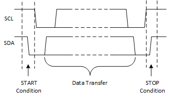 Figure 22. Definition of START and STOP Conditions
7.5.1.3 Data Validity and Byte Formation
One data bit is transferred during each clock pulse of the SCL. One byte is comprised of eight bits on the SDA line. A byte may either be a device address, register address, or data written to or read from a slave.
Data is transferred Most Significant Bit (MSB) first. Any number of data bytes can be transferred from the master to slave between the START and STOP conditions. Data on the SDA line must remain stable during the high phase of the clock period, as changes in the data line when the SCL is high are interpreted as control commands (START or STOP).
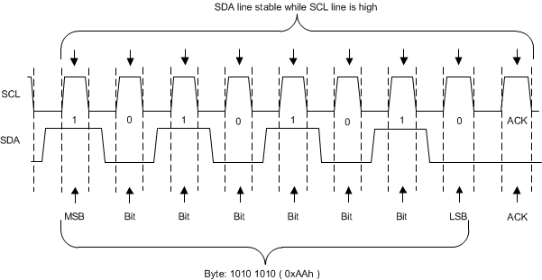 Figure 23. Definition of Byte Formation
7.5.1.4 Acknowledge (ACK) and Not Acknowledge (NACK)
Each byte is followed by one ACK bit from the receiver. The ACK bit allows the receiver to communicate to the transmitter that the byte was successfully received and another byte may be sent.
The transmitter must release the SDA line before the receiver can send the ACK bit. To send an ACK bit, the receiver shall pull down the SDA line during the low phase of the ACK/NACK-related clock period (period 9), so that the SDA line is stable low during the high phase of the ACK/NACK-related clock period. Setup and hold times must be taken into account.
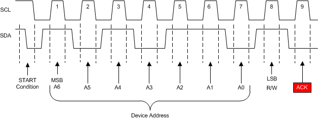 Figure 24. Example use of ACK
When the SDA line remains high during the ACK/NACK-related clock period, this is a NACK signal. There are several conditions that lead to the generation of a NACK:
- The receiver is unable to receive or transmit because it is performing some real-time function and is not ready to start communication with the master.
- During the transfer, the receiver gets data or commands that it does not understand.
- During the transfer, the receiver cannot receive any more data bytes.
- A master-receiver is done reading data and indicates this to the slave through a NACK.
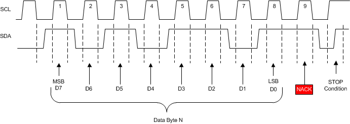 Figure 25. Example use of NACK
7.5.2 I2C Write and Read Operation
7.5.2.1 Auto Increment Function
Auto increment allows multiple bytes to be written to or read from consecutive registers without requiring the master to repeatedly send the device address and register address for each data byte. This is beneficial because auto increment substantially reduces the number of bytes transferred between the master and slave.
For the TPL0102, the registers will auto increment as long as the user continues to enter data. Auto increment will stop once the user is finished entering data bytes.
If there are more bytes to write or read after the last register address is written to or read from in the register map, auto increment will loop around to the register address at the beginning of the register map. For example, after the ACR (register address 0x10h) has been written to, if there are more bytes to be written, the register address will loop to the IVRA (register address 0x00h) at the beginning of the register map.
7.5.2.2 Write Operation
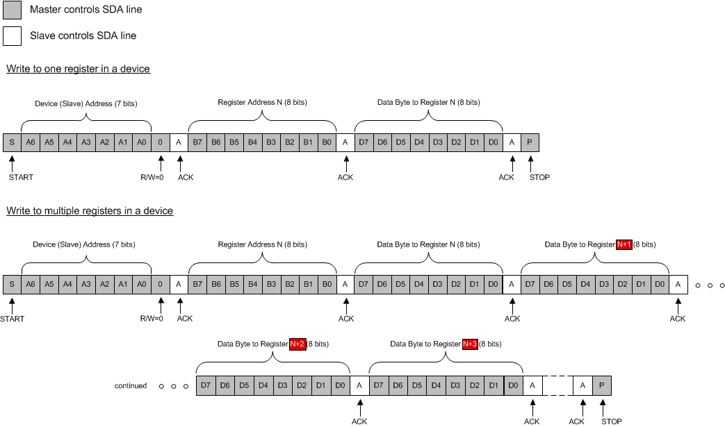 Figure 26. Write Operation to One or Multiple Registers
7.5.2.3 Repeated Start
A repeated START condition may be used in place of a complete STOP condition follow by another START condition when performing a read function. The advantage of this is that the I2C bus does not become available after the stop and therefore prevents other devices from grabbing the bus between transfers.
7.5.2.4 Read Operation
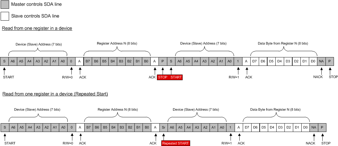 Figure 27. Read Operation from One Register
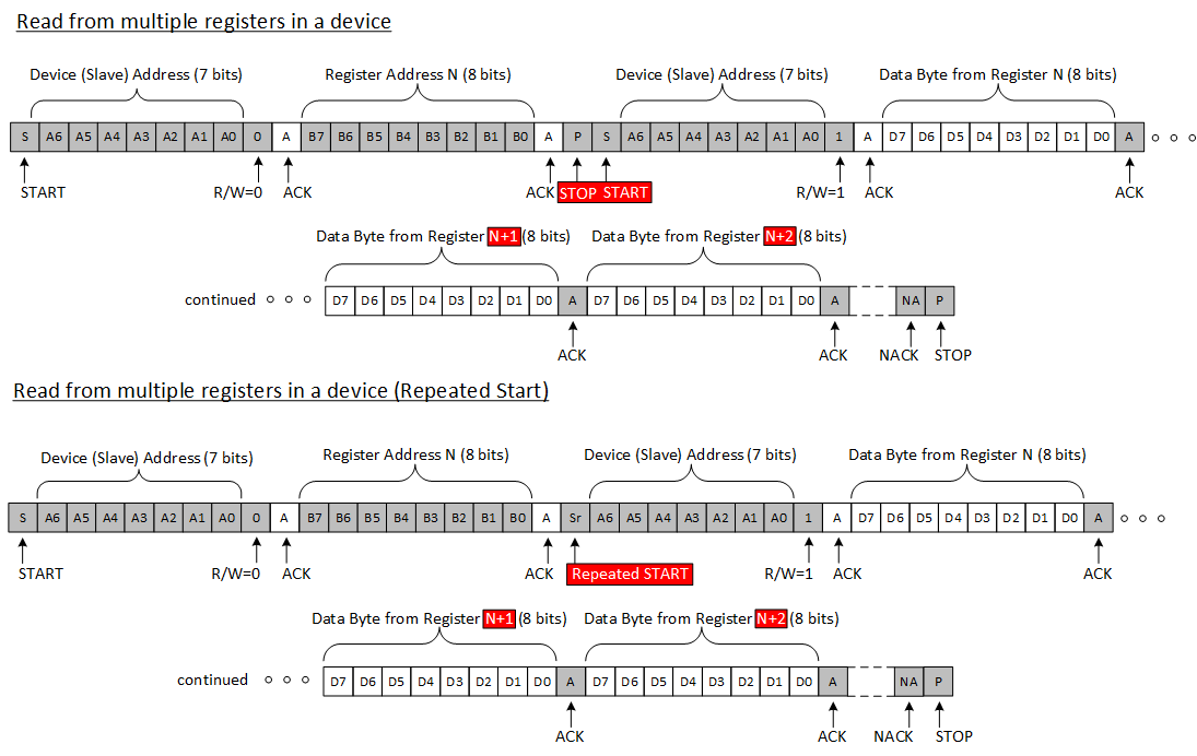 Figure 28. Read Operation from Multiple Registers
7.6 Register Maps
7.6.1 Slave Address
The device (slave) address can be configured by the user with 3 bits (A2, A1, and A0), allowing for 8 different possibilities for the device address. Please see the Figure 30 for an example.
 Figure 29. Device Address in Context with START and ACK
| Bit 7 (MSB) |
Bit 6 | Bit 5 | Bit 4 | Bit 3 | Bit 2 | Bit 1 | Bit 0 (LSB) |
|---|---|---|---|---|---|---|---|
| 1 | 0 | 1 | 0 | A2 | A1 | A0 | R/W |
Figure 30 shows an example of how to configure A2, A1 and A0 to give unique device addresses on the same I2C bus. When a bit is wired to Vcc, this gives that bit a value of 1. When a bit is wired to GND, this gives that bit a value of 0.
For example, Device 1 could be the TPL0102 on the I2C bus, which would have a 7 bit device address of 1010 110. There are some interfaces that will require the device address to be inputted in hex. In order to make the device address 8 bits for hex notation, a leading 0 is added to the left of the 7 bit device address. For Device 1, the 8 bit device address is 0101 0110 (0x56h). Device 2 would have a 7 bit device address of 1010 100, which with a leading 0 results in an 8 bit device address of 0101 0100 (0x54h). Device 3 would have a 7 bit device address of 1010 011, and with a leading 0 results in an 8 bit device address of 0101 0011 (0x53h).
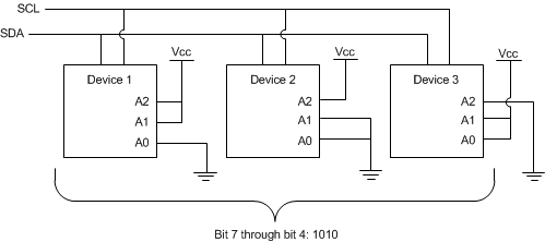 Figure 30. Examples of Device Address Configuration on I2C Bus
7.6.2 TPL0102 Register Map
- When writing the entire register map using auto increment, general purpose registers in the register address map need to be written with dummy bytes. The general purpose registers do not effect the outputs of the potentiometers.
- As stated in the Overview, the VOL bit from the ACR (Access Control Register) provides two options for register accessibility. Either only volatile registers (WR) are accessible to change the wiper setting without storing the value in non-volatile memory or volatile registers (WR) and non-volatile registers (IVR) are accessible to change the wiper setting, which allows the value to be stored in non-volatile memory.
- The respective non-volatile and volatile registers have the same register address, thus to write to both the volatile and non-volatile locations, only one register address needs to be entered and the VOL bit needs to be configured properly.
| REGISTER ADDRESS (HEX) | REGISTER ADDRESS (BINARY) | NON-VOLATILE | VOLATILE |
|---|---|---|---|
| 0x00h | 0000 0000 | IVRA | WRA |
| 0x01h | 0000 0001 | IVRB | WRB |
| 0x02h | 0000 0010 | General purpose | N/A |
| 0x03h | 0000 0011 | General purpose | N/A |
| 0x04h | 0000 0100 | General purpose | N/A |
| 0x05h | 0000 0101 | General purpose | N/A |
| 0x06h | 0000 0110 | General purpose | N/A |
| 0x07h | 0000 0111 | General purpose | N/A |
| 0x08h | 0000 1000 | General purpose | N/A |
| 0x09h | 0000 1001 | General purpose | N/A |
| 0x0Ah | 0000 1010 | General purpose | N/A |
| 0x0Bh | 0000 1011 | General purpose | N/A |
| 0x0Ch | 0000 1100 | General purpose | N/A |
| 0x0Dh | 0000 1101 | General purpose | N/A |
| 0x0Eh | 0000 1110 | General purpose | N/A |
| 0x0Fh | 0000 1111 | Reserved | |
| 0x10h | 0001 0000 | N/A | ACR |
7.6.3 IVRA (Initial Value Register for Potentiometer A)
- Non-volatile register to store wiper position for potentiometer A
- Register will hold value even when device is powered down
| NAME | TYPE | SIZE (BITS) | REGISTER ADDRESS | FACTORY PROGRAMMED VALUE |
|---|---|---|---|---|
| IVRA | Non-volatile Write/Read | 8 | 0x00h | 0x80h |
7.6.4 WRA (Wiper Resistance Register for Potentiometer A)
- Volatile register to change wiper position for potentiometer A
- IVRA loads value to WRA to determine wiper position
| NAME | TYPE | SIZE (BITS) | REGISTER ADDRESS | VALUE UPON RESET |
|---|---|---|---|---|
| WRA | Volatile Write/Read | 8 | 0x00h | IVRA value |
7.6.5 IVRB (Initial Value Register for Potentiometer B)
- Non-volatile register to store wiper position for potentiometer B
- Register will hold value even when device is powered down
| NAME | TYPE | SIZE (BITS) | REGISTER ADDRESS | FACTORY PROGRAMMED VALUE |
|---|---|---|---|---|
| IVRB | Non-volatile Write/Read | 8 | 0x01h | 0x80h |
7.6.6 WRB (Wiper Resistance Register for Potentiometer B)
- Volatile register to change wiper position for potentiometer B
- IVRB loads value to WRB to determine wiper position
| NAME | TYPE | SIZE (BITS) | REGISTER ADDRESS | VALUE UPON RESET |
|---|---|---|---|---|
| WRB | Volatile Write/Read | 8 | 0x01h | IVRB value |
7.6.7 ACR (Access Control Register)
- Volatile register to control register access, determine shut-down mode, and read non-volatile write operations
| NAME | TYPE | SIZE (BITS) | REGISTER ADDRESS | VALUE UPON RESET |
|---|---|---|---|---|
| ACR | Volatile Write/Read | 8 | 0x10h | 0x40h |
| NAME | BIT ASSIGNMENT | ||||||||
|---|---|---|---|---|---|---|---|---|---|
| ACR | Bit 7 | Bit 6 | Bit 5 | Bit 4 | Bit 3 | Bit 2 | Bit 1 | Bit 0 | |
| VOL | SHDN | WIP | 0 | 0 | 0 | 0 | 0 | ||
| Reset (Default) Value | 0 | 1 | 0 | 0 | 0 | 0 | 0 | 0 | |
| NAME | TYPE | SIZE (BITS) | BIT VALUE | DESCRIPTION | ||
|---|---|---|---|---|---|---|
| VOL | Volatile Write/Read | 1 | 0 | Non-volatile registers (IVRA, IVRB) are accessible. Value written to IVR register is also written to the corresponding WR. If read operation is performed, only non-volatile register (IVRA, IVRB) values will be reported. | ||
| 1 | Only Volatile Registers (WR) are accessible. If read operation is performed, only volatile (WRA, WRB) values will be reported. | |||||
| SHDN | Volatile Write/Read | 1 | 0 | Shutdown mode is enabled. Both potentiometers are in shutdown mode. (see Shutdown Mode) | ||
| 1 | Shutdown mode is disabled | |||||
| WIP | Volatile Read | 1 | 0 | Non-volatile write operation is not in progress | ||
| 1 | Non-volatile write operation is in progress (it is not possible to write to the WR or ACR while WIP = 1) | |||||