ZHCSE79C March 2011 – September 2015
PRODUCTION DATA.
- 1 特性
- 2 应用
- 3 说明
- 4 修订历史记录
- 5 Pin Configuration and Functions
- 6 Specifications
-
7 Detailed Description
- 7.1 Overview
- 7.2 Functional Block Diagram
- 7.3 Feature Description
- 7.4 Device Functional Modes
- 7.5 Programming with I2C
- 7.6
Register Maps
- 7.6.1 Slave Address
- 7.6.2 TPL0102 Register Map
- 7.6.3 IVRA (Initial Value Register for Potentiometer A)
- 7.6.4 WRA (Wiper Resistance Register for Potentiometer A)
- 7.6.5 IVRB (Initial Value Register for Potentiometer B)
- 7.6.6 WRB (Wiper Resistance Register for Potentiometer B)
- 7.6.7 ACR (Access Control Register)
- 8 Application and Implementation
- 9 Power Supply Recommendations
- 10Layout
- 11器件和文档支持
- 12机械、封装和可订购信息
封装选项
机械数据 (封装 | 引脚)
散热焊盘机械数据 (封装 | 引脚)
- RUC|14
订购信息
8 Application and Implementation
NOTE
Information in the following applications sections is not part of the TI component specification, and TI does not warrant its accuracy or completeness. TI’s customers are responsible for determining suitability of components for their purposes. Customers should validate and test their design implementation to confirm system functionality.
8.1 Application Information
There are many applications in which variable resistance or voltage division is needed through the use of a digital potentiometer such as the TPL0102; these are just a few examples. In conjunction with various amplifiers, the TPL0102 can effectively be used in rheostat mode to modify the gain of an amplifier, in voltage divider mode to create a Digital to Analog Converter, or one of the potentiometers can be used in voltage divider mode while the other is in rheostat mode to create a variable current sink.
8.2 Typical Applications
8.2.1 Adjustable Gain Non-Inverting Amplifier
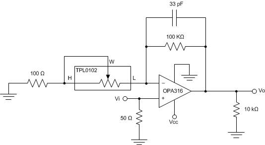 Figure 31. Gain Control Compensation Schematic
8.2.1.1 Design Requirements
| DESIGN PARAMETER | EXAMPLE VALUE |
|---|---|
| Gain range | 6 to 60 dB |
8.2.1.2 Detailed Design Procedure
The TPL0102 can be used in rheostat mode with an OPA316 to create an adjustable gain non-inverting amplifier. The capacitor and resistor values were chosen based upon the Non-Inverting Amplifier Gain equation:

Where Zin is the impedance between the inverting input and GND and Zf is the impedance of the feedback network.
In this application, the following equations are used:

and

Where Rf and Cf are the feedback resistor and capacitor, respectively.
A 100 Ω resistor is added in series with the TPL0102 resistance in order to stop the op amp from producing infinite gain. When the TPL0102 is at zero-scale, the resistance between terminal L and terminal W is ~0 Ω. This would normally cause infinite gain, but with the 100 Ω resistor is series, the lowest Zin can be is 100 Ω, which at DC will create a gain of roughly 60 dB.

Rf and Cf were chosen based upon characteristics of the potentiometer and op amp, respectively. The value of Rf affects the level of gain, primarily at low frequencies. Since the TPL0102 has a full-scale resistance of 100 kΩ between terminal W and terminal L, the Rf was chosen to match this full-scale resistance, which produces the minimum gain of 6 dB:

As frequency increases, Cf begins to have an impact on gain. A frequency roll-off will occur due to the open-loop gain of the op amp, but in this application, the desired effect is to have Cf impact the roll off before the open loop gain of the op amp. At a gain of 40 dB, the op amp open loop gain will force the roll off to occur at 100 kHz. Therefore, in order for Cf to impact the roll off before the open loop gain, roll off due to the capacitor must occur at less than 100 kHz. In this application, 50 kHz is the desired roll off frequency, resulting in a Cf value of 33 pF.

Measurements were taken with a 10 kΩ load. A 50 Ω resistor is included at the input for termination of measurement equipment.
8.2.1.3 Application Curves
As the TPL0102 moves from full-scale to zero-scale, Zin decreases, which causes the gain of the op amp to increase from 6 dB to 56 dB. The amplifier does not reach the full 60 dB of calculated gain because the resistance in the TPL0102 did not reach 0 Ω. At zero-scale, the TPL0102 had a remaining resistance of approximately 58 Ω.

The application curve clearly shows the effect of the low pass filter created by the Rf and Cf combination. Roll off begins as frequencies approach 50 kHz because of the pole created by the 33 pF capacitor. As the frequency increases beyond 50 kHz, the gain decreases by -20 dB/dec until the gain levels off at 1V/V or 0dB. The gain levels off due to the nature of non-inverting op amp transfer functions. The feedback impedance, Zf, is approximately zero at high frequency because Cf acts as a short. As shown below, this results in a gain of 0 dB:

At approximately 3 MHz, the gain is again reduced by –20 dB/dec due to the pole created by open-loop gain of the OPA316.
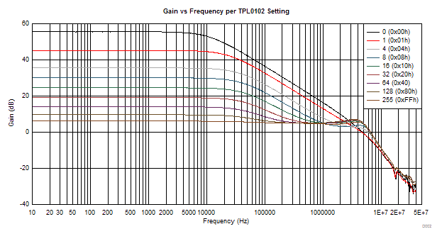 Figure 32. Gain vs Frequency
8.2.2 Digital to Analog Converter (DAC)
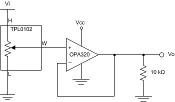 Figure 33. Digital to Analog Converter Schematic
8.2.2.1 Design Requirements
| DESIGN PARAMETER | EXAMPLE VALUE |
|---|---|
| Input Voltage Range | 0 to 5 V |
| Output Voltage Range | 0 to 5 V |
8.2.2.2 Detailed Design Procedure
The TPL0102 can be used in voltage divider mode with a unity-gain op amp buffer to create an 8-bit Digital to Analog Converter (DAC). The analog output voltage of the circuit is determined by the wiper setting programmed through the I2C bus.
The op amp is required to buffer the high-impedance output of the TPL0102 or else loading placed on the output of the voltage divider will affect the output voltage.
8.2.2.3 Application Curves
The voltage at terminal H determines the maximum analog voltage at the output. As the TPL0102 moves from zero-scale to full-scale, the voltage divider adjusts with relation to the voltage divider formula (Equation 1), resulting in the desired voltage at terminal W. The voltage at terminal W will range linearly from 0 V to the terminal H voltage. In this example, Vin at terminal H is 5 V and 2.7 V.
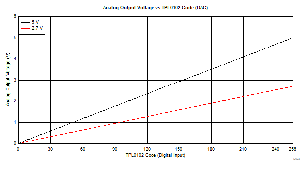 Figure 34. TPL0102 Digital Input vs OPA320 Analog Output (DAC)
8.2.3 Variable Current Sink
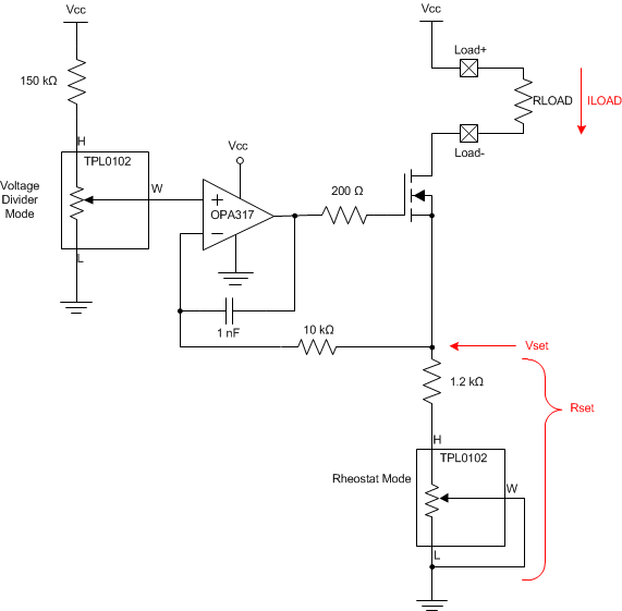 Figure 35. Variable Current Sink Schematic
8.2.3.1 Design Requirements
| DESIGN PARAMETER | EXAMPLE VALUE |
|---|---|
| Load Current Range | 0 µA to 1.33 mA |
8.2.3.2 Detailed Design Procedure
Both potentiometers within the TPL0102 can be used with an OPA317 op amp and N-Channel MOSFET to produce a variable current sink. The first potentiometer, configured in voltage divider mode, is used to set the input voltage to the OPA317. The second potentiometer, configured in rheostat mode, is used to set the span of the current (ILOAD) running through RLOAD. The load current for the circuit is shown below:

Based upon the voltage divider formula between the setting of the TPL0102 and the 150 kΩ resistor, the voltage at the positive input of the OPA317, Vset, can range from 0 to 2 V. This leaves a maximum of 3 V of voltage drop from the positive side to the negative side of the external load with a 5 V supply. A 1.2 kΩ resistor is placed in series with the TPL0102 span setting potentiometer (Rset). At full scale of the span setting potentiometer and the maximum voltage at Vset (2 V), the maximum value for ILOAD is:

When the span setting potentiometer is at zero scale with the maximum voltage at Vset, the maximum value for ILOAD is:

The same calculations can be made when the potentiometer in voltage divider mode is a zero scale. At zero scale, Vset will be almost negligible, resulting in 0 A of current no matter the value of the span setting potentiometer.
8.2.3.2.1 Compensation Components
This design requires a few compensation components to stabilize the feedback network. These include the 1 nF capacitor and the 200 Ω and 10 kΩ resistors, which were selected based upon the TIPD102 reference design.
8.2.3.3 Application Curves
As the TPL0102 in rheostat mode (span setting potentiometer) moves from zero-scale to full-scale, a new step (line) is created with a larger achievable maximum current. The rheostat mode potentiometer directly corresponds to Rset in Equation 13. The TPL0102 in voltage divider mode produces the granular current values between the minimum and maximum range. The voltage divider potentiometer directly corresponds to Vset in Equation 13. For example, when the potentiometer in rheostat mode is at code 256, the potentiometer in voltage divider mode produces a theoretical maximum current of 1.33 mA at code 256 and a minimum current of 0 µA at code 0.
The current sink does not reach the full 1.33 mA because of the error in resistance of the span setting potentiometer. At full-scale, the resistor had an actual resistance of 480 Ω.

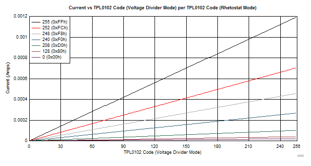 Figure 36. Current vs Span Setting Code