SLRS066D January 2014 – March 2016 TPL7407L
PRODUCTION DATA.
- 1 Features
- 2 Applications
- 3 Description
- 4 Revision History
- 5 Pin Configuration and Functions
- 6 Specifications
- 7 Detailed Description
- 8 Application and Implementation
- 9 Power Supply Recommendations
- 10Layout
- 11Device and Documentation Support
- 12Mechanical, Packaging, and Orderable Information
8 Application and Implementation
NOTE
Information in the following applications sections is not part of the TI component specification, and TI does not warrant its accuracy or completeness. TI’s customers are responsible for determining suitability of components for their purposes. Customers should validate and test their design implementation to confirm system functionality.
8.1 Application Information
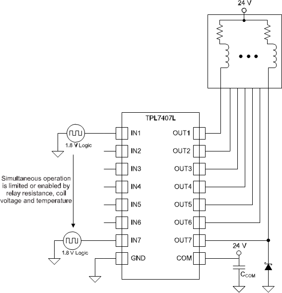
TPL7407L will typically be used to drive a high voltage and/or current peripheral from an MCU or logic device that cannot tolerate these conditions. The following design is a common application of TPL7407L, driving inductive loads. This includes motors, solenoids & relays. Each load type can be modeled by what's seen in Figure 9.
8.2 Typical Application
8.2.1 Inductive Load Driver
Please note that inductive loads, such as stepper motors or relays, can generate negative transients on the OUTx pins of the device. Typically this occurs when the output channel FET turns ON, pulling the OUTx node to ground. This can cause the OUTx node to go below the voltage rating listed in the Absolute Maximum Ratings table, which in effect causes excessive ground current leakage. This effect is only seen on the OUT7 pin, and prolonged usage in this condition can cause permanent damage to the device.
If the application has an inductive load connected to OUT7, it is recommended to use an external Schottky diode to protect the OUT7 pin from negative transients larger than those listed in the Absolute Maximum Ratings table, such as in Figure 9 below.
8.2.1.1 Design Requirements
For this design example, use the parameters listed in Table 1 as the input parameters.
Table 1. Design Parameters
| DESIGN PARAMETER | EXAMPLE VALUE |
|---|---|
| GPIO Voltage | 1.8 V, 3.3 V or 5.0 V |
| Coil Supply Voltage | 8.5 V to 40 V |
| Number of Channels | 7 |
| Output Current (RCOIL) | 20 mA to 300 mA per channel |
| CCOM | 0.1 µF |
| Duty Cycle | 100% |
8.2.1.2 Detailed Design Procedure
When using TPL7407L in a coil driving application, determine the following:
- Input Voltage Range
- Temperature Range
- Output & Drive Current
- Power Dissipation
8.2.1.2.1 TTL and other Logic Inputs
TPL7407L input interface is specified for standard 1.8 V through 5 V CMOS logic interface and can tolerate up to 30 V. At any input voltage the output drivers will be driven at it's maximum when Vcom is greater than or equal to 8.5 V.
8.2.1.2.2 Input RC Snubber
TPL7407L features an input RC snubber that helps prevent spurious switching in noisy environments. Connect an external 1 kΩ to 5 kΩ resistor in series with the input to further enhance TPL7407L’s noise tolerance.
8.2.1.2.3 High-impedance Input Drivers
TPL7407L features a 1-MΩ input pull-down resistor. The presence of this resistor allows the input drivers to be tri-stated. When a high-impedance driver is connected to a channel input the TPL7407L detects the channel input as a low level input and remains in the OFF position. The input RC snubber helps improve noise tolerance when input drivers are in the high-impedance state.
8.2.1.2.4 Drive Current
The coil current is determined by the coil voltage (VSUP), coil resistance & output low voltage (VOL).
8.2.1.2.5 Output Low Voltage
The output low voltage (VOL) is drain to source (VDS) voltage of the output NMOS transistors when the input is driven high and it is sinking current and can be determined by Specifications or Figure 1.
8.2.1.3 Application Curves
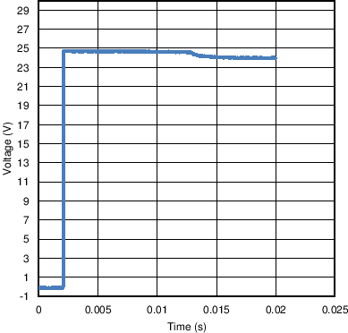
The following curve was generated with TPL7407L driving an OMRON G5NB relay -- Vin = 5.0 V; Vsup = 24 V & RCOIL = 2.8 kΩ
 Figure 10. Output Response With De-activation of Coil (Turn Off)
8.2.2 Unipolar Stepper Motor Driver
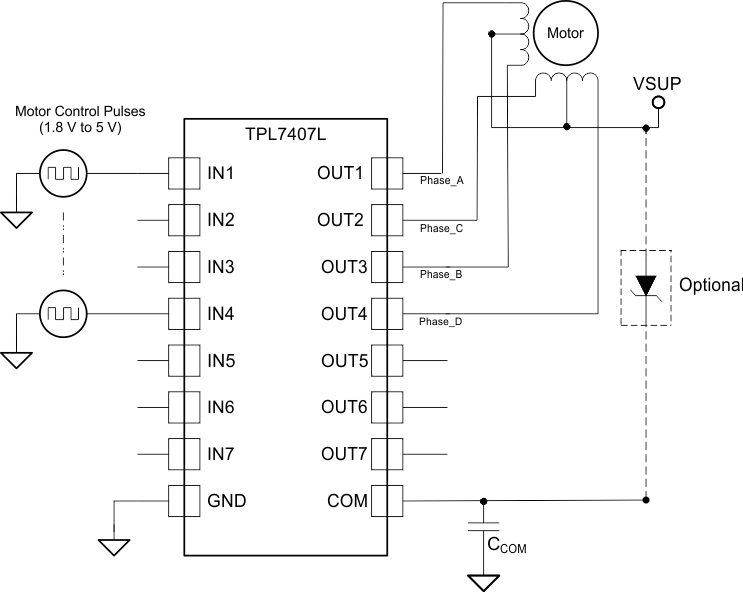
 Figure 11. Stepper Motor Driver Schematic
8.2.2.1 Design Requirements
Figure 11 shows an implementation of TPL7407L for driving a uniploar stepper motor. The unconnected input channels can be used for other functions. When an input pin is left open the internal 1 MΩ pull down resistor pulls the respective input pin to GND potential. For higher noise immunity use an external short across an unconnected input and GND pins. The COM pin must be tied to the supply of whichever inductive load is being driven for the driver to be protected by the free-wheeling diode.
Whenever a Zener diode is used between Vcom and the motor supply, the Vcom pin will slew from the coil supply to a voltage that is the sum of the Zener voltage and the coil supply when there is a flyback event. Depending on the coil inductance and resistance, this can be very rapid. Whenever the COM pin experiences a slew rate greater than 0.5 V/µs, a capacitor must be added to limit the slew to < 0.5 V/µs. See Power Supply Recommendations for further explanation.
8.2.2.2 Detailed Design Procedure
Refer to Design Requirements.
8.2.2.3 Application Curves
Refer to Thermal Characteristics.
8.2.3 Multi-Purpose Sink Driver
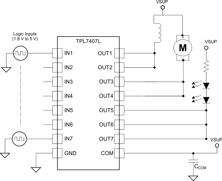
 Figure 12. Multi-Purpose Sink Driver Schematic
8.2.3.1 Design Requirements
When configured as per Figure 12 TPL7407L may be used as a multi-purpose driver. The output channels may be tied together to sink more current. TPL7407L can easily drive motors, relays & LEDs with little power dissipation. COM must be tied to highest load voltage, which may or may not be same as inductive load supply.
8.2.3.2 Detailed Design Procedure
Refer to Design Requirements.
8.2.3.3 Application Curves
Refer to Thermal Characteristics.
