ZHCSQN1 October 2023 TPS1210-Q1
ADVANCE INFORMATION
- 1
- 1 特性
- 2 应用
- 3 说明
- 4 Revision History
- 5 Device Comparison
- 6 Pin Configuration and Functions
- 7 Specifications
- 8 Parameter Measurement Information
-
9 Detailed Description
- 9.1 Overview
- 9.2 Functional Block Diagram
- 9.3
Feature Description
- 9.3.1 Charge Pump and Gate Driver Output (VS, G1PU, G1PD, G2, BST, SRC)
- 9.3.2 Capacitive Load Driving Using FET Gate (G1PU, G1PD) Slew Rate Control
- 9.3.3 Short-Circuit Protection
- 9.3.4 Undervoltage Protection (UVLO)
- 9.3.5 Reverse Polarity Protection
- 9.3.6 Short-Circuit Protection Diagnosis (SCP_TEST)
- 9.3.7 TPS1210x-Q1 as a Simple Gate Driver
- 9.4 Device Functional Modes
- 10Application and Implementation
- 11Device and Documentation Support
- 12Mechanical, Packaging, and Orderable Information
10.2.3 Application Curves
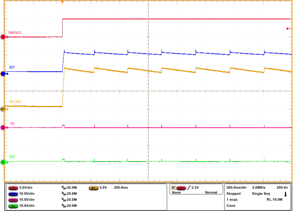 Figure 10-2 Start-Up Profile of Bootstrap Voltage with INP1=INP2 = GND and CBST = 470 nF
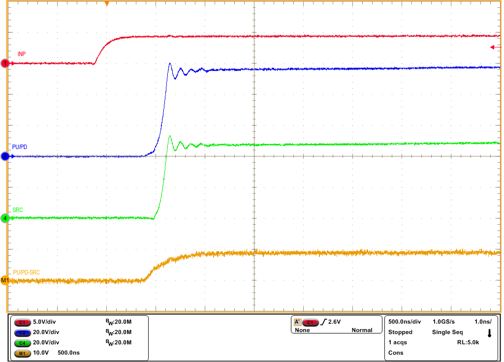 Figure 10-4 Turn-ON Response of TPS12100-Q1 for INP1 -> LOW to HIGH and CBST = 470 nF
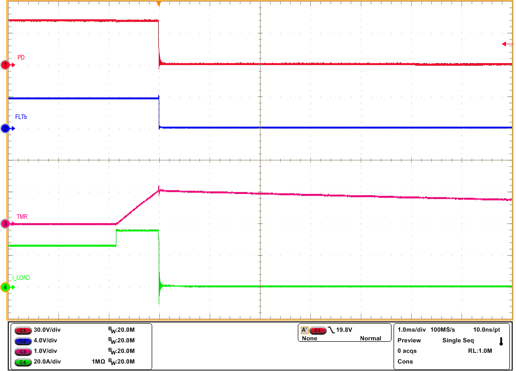 Figure 10-6 Overcurrent Response of TPS12100-Q1 for a Load Step from 25 A to 35 A with 30-A Overcurrent Protection Setting
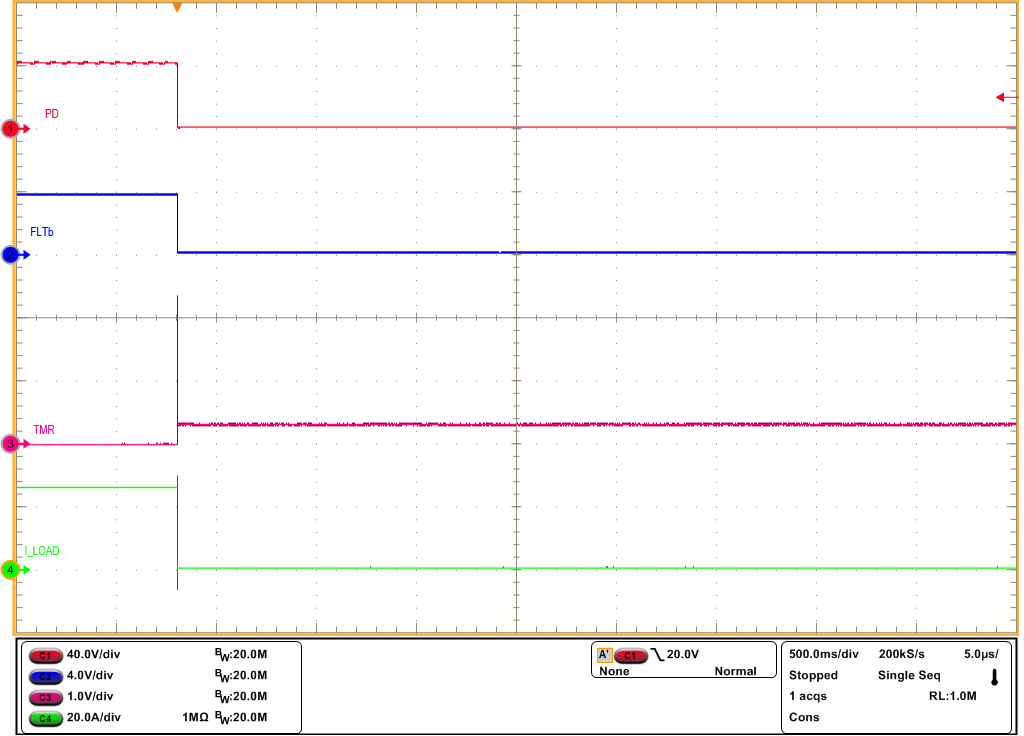 Figure 10-8 Latch-Off Response of TPS12100-Q1 for an Overcurrent Fault
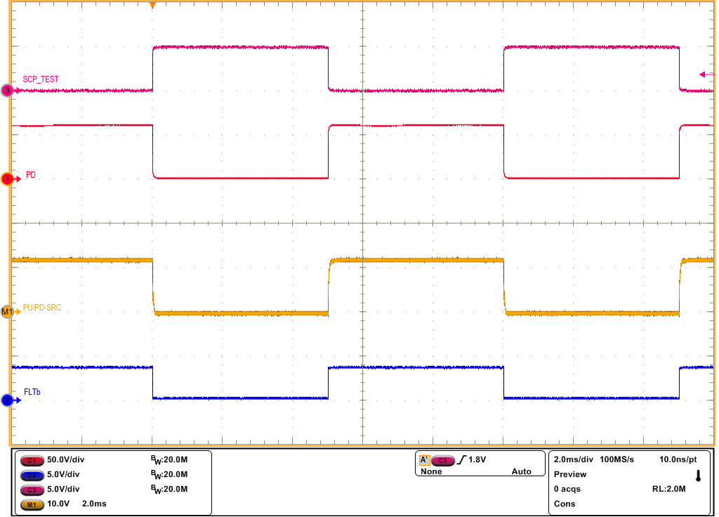 Figure 10-10 Short-Circuit Protection Diagnosis Test Response of TPS12100-Q1
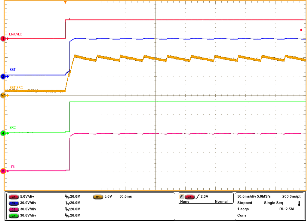 Figure 10-3 Start-Up Profile of Bootstrap Voltage with INP1=INP2 = HIGH and CBST = 470 nF
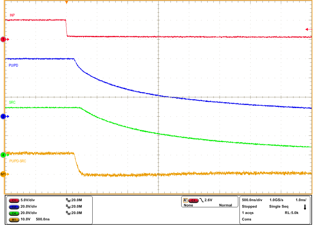 Figure 10-5 Turn-OFF Response of TPS12100-Q1 for INP1 -> HIGH to LOW and CBST = 470 nF
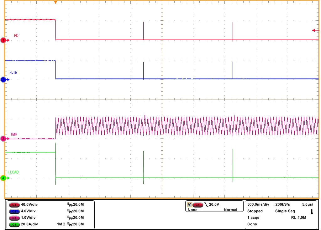 Figure 10-7 Auto-Retry Response of TPS12100-Q1 for an Overcurrent Fault
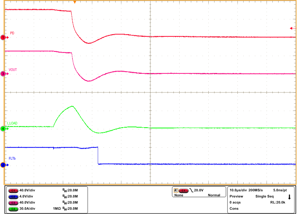 Figure 10-9 Output Short-Circuit Response of TPS12100-Q1 Device