ZHCSNE6 August 2021 TPS1653
PRODUCTION DATA
- 1 特性
- 2 应用
- 3 说明
- 4 Revision History
- 5 Pin Configuration and Functions
- 6 Specifications
- 7 Parameter Measurement Information
-
8 Detailed Description
- 8.1 Overview
- 8.2 Functional Block Diagram
- 8.3
Feature Description
- 8.3.1 Hot Plug-In and In-Rush Current Control
- 8.3.2 Undervoltage Lockout (UVLO)
- 8.3.3 Overload and Short Circuit Protection
- 8.3.4 Current Monitoring Output (IMON)
- 8.3.5 FAULT Response (FLT)
- 8.3.6 Power Good Output (PGOOD)
- 8.3.7 IN, P_IN, OUT and GND Pins
- 8.3.8 Thermal Shutdown
- 8.3.9 Low Current Shutdown Control (SHDN)
- 8.3.10 Enable Input (EN)
- 8.4 Device Functional Modes
- 9 Application and Implementation
- 10Power Supply Recommendations
- 11Layout
- 12Device and Documentation Support
- 13Mechanical, Packaging, and Orderable Information
封装选项
机械数据 (封装 | 引脚)
散热焊盘机械数据 (封装 | 引脚)
订购信息
8.3.3.2 Short Circuit Protection
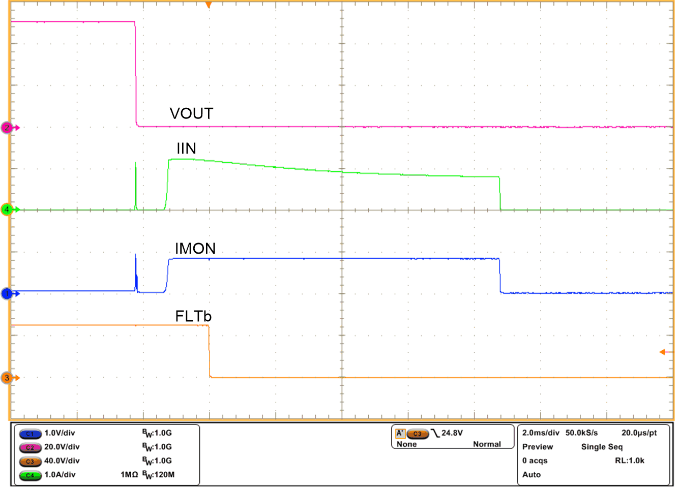
During a transient output short circuit event, the current through the device increases rapidly. As the current-limit amplifier cannot respond quickly to this event due to its limited bandwidth, the device incorporates a fast-trip comparator. The fast-trip comparator architecture is designed for fast turn OFF tFASTTRIP(dly) = 1 µs (typical) with I(SCP) = 45 A of the internal FET during an output short circuit event. The fast-trip threshold is internally set to I(FASTTRIP). The fast-trip circuit holds the internal FET off for only a few microseconds, after which the device turns back on slowly, allowing the current-limit loop to regulate the output current to I(OL). Then the device functions similar to the overload condition. Figure 8-5 illustrates output hot-short performance of the device.

| VIN = 50 V | RILIM = 18 kΩ |
The fast-trip comparator architecture has a supply line noise immunity resulting in a robust performance in noisy environments. This performance is achieved by controlling the turn OFF time of the internal FET based on the overcurrent level, I(FASTTRIP), through the device. The higher the overcurrent, the faster the turn OFF time, tFASTTRIP(dly). At Overload current level in the range of IFASTTRIP < IOUT < ISCP, the fast-trip comparator response is 3.2 µs (typical).