ZHCSIV1F September   2018  – February 2023 TPS1663

PRODUCTION DATA  

  1. 特性
  2. 应用
  3. 说明
  4. Revision History
  5. Device Comparison Table
  6. Pin Configuration and Functions
  7. Specifications
    1. 7.1 Absolute Maximum Ratings
    2. 7.2 ESD Ratings
    3. 7.3 Recommended Operating Conditions
    4. 7.4 Thermal Information
    5. 7.5 Electrical Characteristics
    6. 7.6 Timing Requirements
    7. 7.7 Typical Characteristics
  8. Parameter Measurement Information
  9. Detailed Description
    1. 9.1 Overview
    2. 9.2 Functional Block Diagram
    3. 9.3 Feature Description
      1. 9.3.1  Hot Plug-In and In-Rush Current Control
        1. 9.3.1.1 Thermal Regulation Loop
      2. 9.3.2  Undervoltage Lockout (UVLO)
      3. 9.3.3  Overvoltage Protection (OVP)
      4. 9.3.4  Overload and Short Circuit Protection
        1. 9.3.4.1 Overload Protection
        2. 9.3.4.2 Short Circuit Protection
          1. 9.3.4.2.1 Start-Up With Short-Circuit On Output
      5. 9.3.5  Output Power Limiting, PLIM (TPS16632 Only)
      6. 9.3.6  Current Monitoring Output (IMON)
      7. 9.3.7  FAULT Response (FLT)
      8. 9.3.8  Power Good Output (PGOOD)
      9. 9.3.9  IN, P_IN, OUT and GND Pins
      10. 9.3.10 Thermal Shutdown
      11. 9.3.11 Low Current Shutdown Control (SHDN)
    4. 9.4 Device Functional Modes
  10. 10Application and Implementation
    1. 10.1 Application Information
    2. 10.2 Typical Application
      1. 10.2.1 Design Requirements
      2. 10.2.2 Detailed Design Procedure
        1. 10.2.2.1 Programming the Current-Limit Threshold R(ILIM) Selection
        2. 10.2.2.2 Undervoltage Lockout and Overvoltage Set Point
        3. 10.2.2.3 Setting Output Voltage Ramp Time (tdVdT)
          1. 10.2.2.3.1 Support Component Selections RPGOOD and C(IN)
      3. 10.2.3 Application Curves
    3. 10.3 System Examples
      1. 10.3.1 Simple 24-V Power Supply Path Protection
    4. 10.4 Power Supply Recommendations
      1. 10.4.1 Transient Protection
    5. 10.5 Layout
      1. 10.5.1 Layout Guidelines
      2. 10.5.2 Layout Example
  11. 11Device and Documentation Support
    1. 11.1 Documentation Support
      1. 11.1.1 Related Documentation
    2. 11.2 接收文档更新通知
    3. 11.3 支持资源
    4. 11.4 Trademarks
    5. 11.5 静电放电警告
    6. 11.6 术语表
  12. 12Mechanical, Packaging, and Orderable Information

请参考 PDF 数据表获取器件具体的封装图。

机械数据 (封装 | 引脚)
  • RGE|24
  • PWP|20
散热焊盘机械数据 (封装 | 引脚)

Low Current Shutdown Control (SHDN)

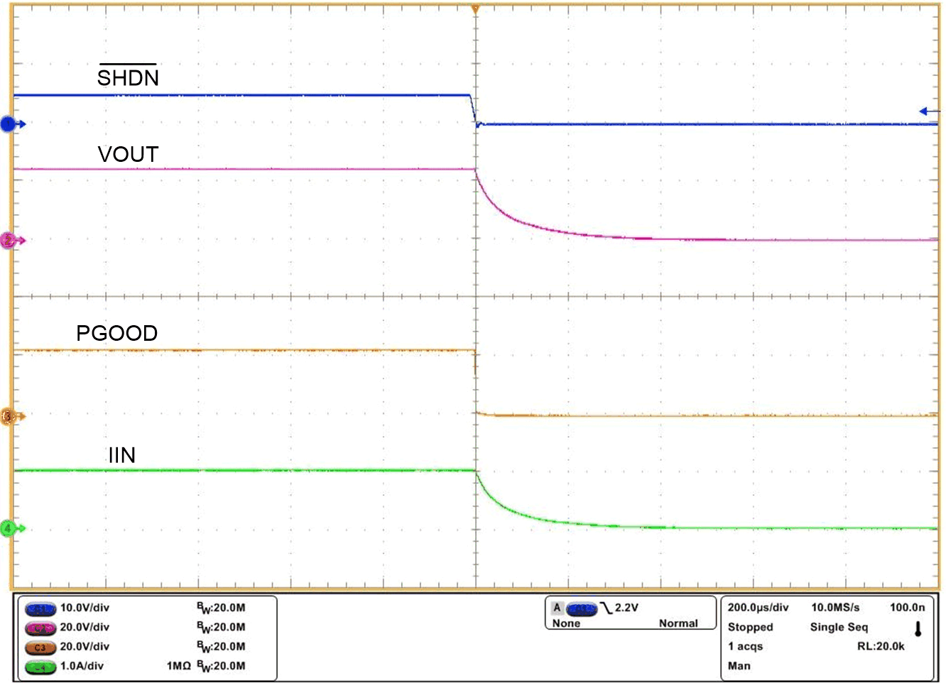
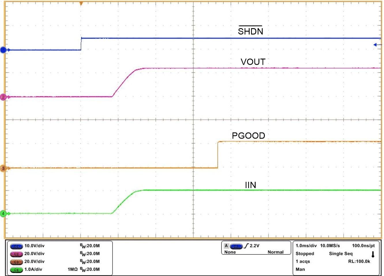
The internal and the external FET and hence the load current can be switched off by pulling the SHDN pin below 0.8-V threshold with a micro-controller GPIO pin or can be controlled remotely with an opto-isolator device. The device quiescent current reduces to 21 μA (typical) in shutdown state. To assert SHDN low, the pull down must have sinking capability of at least 10 µA. To enable the device, SHDN must be pulled up to at least 2 V. Once the device is enabled, the internal FET turns on with dVdT mode.Figure 9-13 and Figure 9-14 illustrate the performance of SHDN control.
GUID-26115B2D-CDBE-4BF6-B595-AC3FBF811249-low.gif
VIN = 24 V C(dVdT) = 22 nF RLOAD = 24 Ω
Figure 9-13 Turnon Control With SHDN
GUID-A4DC5897-BD27-449F-A36E-AFE17232EA0F-low.gif
VIN = 24 V C(dVdT) = 22 nF RLOAD = 24 Ω
Figure 9-14 Turnoff Control With SHDN