ZHCSIV1F September 2018 – February 2023 TPS1663
PRODUCTION DATA
- 1 特性
- 2 应用
- 3 说明
- 4 Revision History
- 5 Device Comparison Table
- 6 Pin Configuration and Functions
- 7 Specifications
- 8 Parameter Measurement Information
-
9 Detailed Description
- 9.1 Overview
- 9.2 Functional Block Diagram
- 9.3
Feature Description
- 9.3.1 Hot Plug-In and In-Rush Current Control
- 9.3.2 Undervoltage Lockout (UVLO)
- 9.3.3 Overvoltage Protection (OVP)
- 9.3.4 Overload and Short Circuit Protection
- 9.3.5 Output Power Limiting, PLIM (TPS16632 Only)
- 9.3.6 Current Monitoring Output (IMON)
- 9.3.7 FAULT Response (FLT)
- 9.3.8 Power Good Output (PGOOD)
- 9.3.9 IN, P_IN, OUT and GND Pins
- 9.3.10 Thermal Shutdown
- 9.3.11 Low Current Shutdown Control (SHDN)
- 9.4 Device Functional Modes
- 10Application and Implementation
- 11Device and Documentation Support
- 12Mechanical, Packaging, and Orderable Information
6 Pin Configuration and Functions
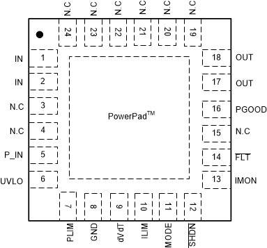
 Figure 6-1 TPS16630 RGE Package,24-Pin VQFN(Top View)
 Figure 6-3 TPS16632 RGE Package,24-Pin VQFN(Top View)
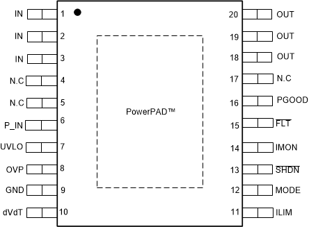
 Figure 6-2 TPS16630 PWP Package,20-Pin HTSSOP(Top View)
Table 6-1 Pin Functions
| PIN | TYPE#GUID-0035D528-587A-47C9-A095-95416BFE3A8A | DESCRIPTION | ||||
|---|---|---|---|---|---|---|
| NAME | TPS16630 | TPS16632 | ||||
| VQFN | HTSSOP | VQFN | ||||
| IN | 1 | 1 | 1 | P | Power input. Connects to the DRAIN of the internal FET. | |
| 2 | 2 | 2 | ||||
| — | 3 | — | ||||
| P_IN | 5 | 6 | 5 | P | Supply voltage of the device. Always connect P_IN to IN directly. | |
| UVLO | 6 | 7 | 6 | I | Input for setting the programmable undervoltage lockout threshold. An undervoltage event turns off the internal FET and asserts FLT to indicate the power-failure. | |
| OVP | 7 | 8 | — | I | Input for setting the adjustable overvoltage protection threshold (for TPS16630 only). An overvoltage event turns off the internal FET and asserts FLT to indicate the overvoltage fault. | |
| PLIM | — | — | 7 | I | Input for setting the adjustable output power limiting threshold (TPS16632 Only). Connect a resistor across PLIM to GND to set the output power limit. Connect PLIM to GND if PLIM feature is not used. See Output Power Limiting, PLIM (TPS16632 Only) section. | |
| GND | 8 | 9 | 8 | — | Connect GND to system ground. | |
| dVdT | 9 | 10 | 9 | I/O | A capacitor from this pin to GND sets output voltage slew rate. Leaving this pin floating enables device power up in thermal regulation resulting in fast output charge. See the Hot Pug-In and In-Rush Current Control section. | |
| ILIM | 10 | 11 | 10 | I/O | A resistor from this pin to GND sets the overload limit. See Overload and Short Circuit Protection section. | |
| MODE | 11 | 12 | 11 | I | Mode selection pin for Overload fault response. See the Device Functional Modes section. | |
| SHDN | 12 | 13 | 12 | I | Shutdown pin. Pulling SHDN low makes the device to enter into low power shutdown mode. Cycling SHDN pin voltage resets the device that has latched off due to a fault condition. | |
| IMON | 13 | 14 | 13 | O | Analog current monitor output. This pin sources a scaled down ratio of current through the internal FET. A resistor from this pin to GND converts current to proportional voltage. If unused, leave it floating. | |
| FLT | 14 | 15 | 14 | O | Fault event indicator. This pin is an open drain output. If unused, leave floating or connect to GND. | |
| PGOOD | 16 | 16 | 16 | O | Active High. A high indicates that the internal FET is enhanced. PGOOD goes low when the internal FET is turned OFF during a fault or when SHDN is pulled low. If PGOOD is unused, then connect to GND or leave it floating. | |
| OUT | 17 | 18 | 17 | P | Power output of the device. | |
| 18 | 19 | 18 | ||||
| — | 20 | — | ||||
| N.C | 3 | 4 | 3 | — | No connect. | |
| 4 | 5 | 4 | ||||
| 15 | 17 | 15 | ||||
| 19 | — | 19 | ||||
| 20 | — | 20 | ||||
| 21 | — | 21 | ||||
| 22 | — | 22 | ||||
| 23 | — | 23 | ||||
| 24 | — | 24 | ||||
| PowerPAD™ | — | Connect PowerPAD to GND plane for heat sinking. Do not use PowerPAD as the only electrical connection to GND. | ||||