ZHCSIV1F September 2018 – February 2023 TPS1663
PRODUCTION DATA
- 1 特性
- 2 应用
- 3 说明
- 4 Revision History
- 5 Device Comparison Table
- 6 Pin Configuration and Functions
- 7 Specifications
- 8 Parameter Measurement Information
-
9 Detailed Description
- 9.1 Overview
- 9.2 Functional Block Diagram
- 9.3
Feature Description
- 9.3.1 Hot Plug-In and In-Rush Current Control
- 9.3.2 Undervoltage Lockout (UVLO)
- 9.3.3 Overvoltage Protection (OVP)
- 9.3.4 Overload and Short Circuit Protection
- 9.3.5 Output Power Limiting, PLIM (TPS16632 Only)
- 9.3.6 Current Monitoring Output (IMON)
- 9.3.7 FAULT Response (FLT)
- 9.3.8 Power Good Output (PGOOD)
- 9.3.9 IN, P_IN, OUT and GND Pins
- 9.3.10 Thermal Shutdown
- 9.3.11 Low Current Shutdown Control (SHDN)
- 9.4 Device Functional Modes
- 10Application and Implementation
- 11Device and Documentation Support
- 12Mechanical, Packaging, and Orderable Information
9.3.2 Undervoltage Lockout (UVLO)
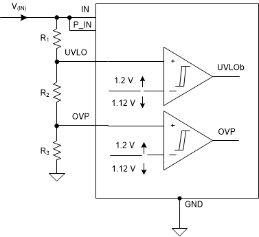
The TPS1663x devices feature an accurate ± 2% adjustable undervoltage lockout functionality. When the voltage at UVLO pin falls below V(UVLOF) during input undervoltage fault, the internal FET quickly turns off and FLT is asserted. The UVLO comparator has a hysteresis of 78 mV (typical). To set the input UVLO threshold, connect a resistor divider network from IN supply to UVLO terminal to GND as shown in Figure 9-3. If the Undervoltage Lockout function is not needed, the UVLO terminal must be connected to the IN terminal. UVLO terminal must not be left floating.
 Figure 9-3 UVLO and OVP Thresholds Set by R1 , R2 and R3