ZHCSH03C August   2017  – June 2019 TPS1H000-Q1

PRODUCTION DATA.  

  1. 特性
  2. 应用
  3. 说明
    1.     Device Images
      1.      典型方框图
      2.      “自动重试”模式下的电流限制保护
  4. 修订历史记录
  5. Pin Configuration and Functions
    1.     Pin Functions
  6. Specifications
    1. 6.1 Absolute Maximum Ratings
    2. 6.2 ESD Ratings
    3. 6.3 Recommended Operating Conditions
    4. 6.4 Thermal Information
    5. 6.5 Electrical Characteristics
    6. 6.6 Switching Characteristics
    7. 6.7 Typical Characteristics
  7. Detailed Description
    1. 7.1 Overview
    2. 7.2 Functional Block Diagram
    3. 7.3 Feature Description
      1. 7.3.1 Current Limit
      2. 7.3.2 DELAY Pin Configuration
        1. 7.3.2.1 Holding Mode
        2. 7.3.2.2 Latch-Off Mode
        3. 7.3.2.3 Auto-Retry Mode
      3. 7.3.3 Standalone Operation
      4. 7.3.4 Fault Truth Table
      5. 7.3.5 Full Diagnostics
        1. 7.3.5.1 Short-to-GND and Overload Detection
        2. 7.3.5.2 Open-Load Detection
          1. 7.3.5.2.1 Output On
          2. 7.3.5.2.2 Output Off
        3. 7.3.5.3 Short-to-Battery Detection
        4. 7.3.5.4 Thermal Fault Detection
          1. 7.3.5.4.1 Thermal Shutdown
          2. 7.3.5.4.2 Thermal Swing
          3. 7.3.5.4.3 Fault Report Holding
      6. 7.3.6 Full Protections
        1. 7.3.6.1 UVLO Protection
        2. 7.3.6.2 Inductive Load Switching Off Clamp
        3. 7.3.6.3 Loss-of-GND Protection
        4. 7.3.6.4 Loss-of-Power-Supply Protection
        5. 7.3.6.5 Reverse-Current Protection
        6. 7.3.6.6 MCU I/O Protection
    4. 7.4 Device Functional Modes
      1. 7.4.1 Working Modes
        1. 7.4.1.1 Normal Mode
        2. 7.4.1.2 Standby Mode
        3. 7.4.1.3 Standby Mode With Diagnostics
  8. Application and Implementation
    1. 8.1 Application Information
    2. 8.2 Typical Application
      1. 8.2.1 Design Requirements
      2. 8.2.2 Detailed Design Procedure
      3. 8.2.3 Application Curves
  9. Power Supply Recommendations
  10. 10Layout
    1. 10.1 Layout Guidelines
    2. 10.2 Layout Example
  11. 11器件和文档支持
    1. 11.1 接收文档更新通知
    2. 11.2 社区资源
    3. 11.3 商标
    4. 11.4 静电放电警告
    5. 11.5 Glossary
  12. 12机械、封装和可订购信息

封装选项

机械数据 (封装 | 引脚)
散热焊盘机械数据 (封装 | 引脚)
订购信息

Reverse-Current Protection

Reverse current occurs in two conditions: short to supply and reverse polarity.

  • When a short to the supply occurs, there is only reverse current through the body diode. IR(1) specifies the limit of the reverse current.
  • In a reverse-polarity condition, there are reverse currents through the body diode and the device GND pin. IR(2) specifies the limit of the reverse current.

To protect the device, TI recommends two types of external circuitry.

  • Adding a blocking diode (method 1). Both the device and load are protected when in reverse polarity.
  • Adding a GND network (method 2). The reverse current through the device GND is blocked. The reverse current through the FET is limited by the load itself. TI recommends a resistor in parallel with the diode as a GND network. The recommended configuration is a 1-kΩ resistor in parallel with a >100-mA diode. The reverse current protection diode in the GND network forward voltage should be less than 0.6 V in any circumstances. In addition a minimum resistance of 4.7 K is recommended on the I/O pins.
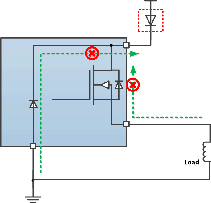
TPS1H000-Q1 Reverse-Blocking-1.gifFigure 29. Reverse-Current External Protection, Method 1
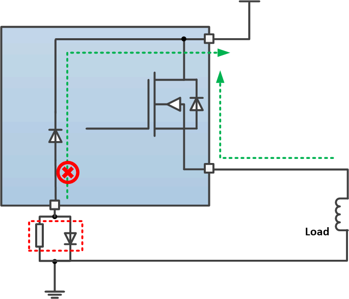
TPS1H000-Q1 Reverse-Blocking-2.gifFigure 30. Reverse-Current External Protection, Method 2