ZHCSHN4D February   2018  – September 2021 TPS1H200A-Q1

PRODUCTION DATA  

  1. 特性
  2. 应用
  3. 说明
  4. Revision History
  5. Pin Configuration and Functions
  6. Specifications
    1. 6.1 Absolute Maximum Ratings
    2. 6.2 ESD Ratings
    3. 6.3 Recommended Operating Conditions
    4. 6.4 Thermal Information
    5. 6.5 Electrical Characteristics
    6. 6.6 Switching Characteristics
    7. 6.7 Typical Characteristics
  7. Detailed Description
    1. 7.1 Overview
    2. 7.2 Functional Block Diagram
    3. 7.3 Feature Description
      1. 7.3.1 Current limit
      2. 7.3.2 DELAY Pin Configuration
        1. 7.3.2.1 Holding Mode
        2. 7.3.2.2 Latch-Off Mode
        3. 7.3.2.3 Auto-Retry Mode
      3. 7.3.3 Stand-alone Operation
      4. 7.3.4 Fault Truth Table
      5. 7.3.5 Full Diagnostics
        1. 7.3.5.1 Short-to-GND and Overload Detection
        2. 7.3.5.2 Open-Load Detection
          1. 7.3.5.2.1 Output On
          2. 7.3.5.2.2 Output Off
        3. 7.3.5.3 Short-to-Battery Detection
        4. 7.3.5.4 Thermal Fault Detection
          1. 7.3.5.4.1 Thermal Shutdown
          2. 7.3.5.4.2 Thermal Swing
          3. 7.3.5.4.3 Fault Report Holding
      6. 7.3.6 Full Protections
        1. 7.3.6.1 UVLO Protection
        2. 7.3.6.2 Inductive Load Switching Off Clamp
        3. 7.3.6.3 Loss-of-GND Protection
        4. 7.3.6.4 Loss-of-Power-Supply Protection
        5. 7.3.6.5 Reverse-Current Protection
        6. 7.3.6.6 MCU I/O Protection
    4. 7.4 Device Functional Modes
      1. 7.4.1 Working Modes
        1. 7.4.1.1 Normal Mode
        2. 7.4.1.2 Standby Mode
        3. 7.4.1.3 Standby Mode With Diagnostics
  8. Application and Implementation
    1. 8.1 Application Information
    2. 8.2 Typical Application
      1. 8.2.1 Design Requirements
      2. 8.2.2 Detailed Design Procedure
      3. 8.2.3 Application Curves
  9. Power Supply Recommendations
  10. 10Layout
    1. 10.1 Layout Guidelines
    2. 10.2 Layout Example
  11. 11Device and Documentation Support
    1. 11.1 Documentation Support
      1. 11.1.1 Related Documentation
    2. 11.2 接收文档更新通知
    3. 11.3 支持资源
    4. 11.4 Trademarks
    5. 11.5 Electrostatic Discharge Caution
    6. 11.6 术语表
  12. 12Mechanical, Packaging, and Orderable Information

封装选项

机械数据 (封装 | 引脚)
散热焊盘机械数据 (封装 | 引脚)
订购信息

Inductive Load Switching Off Clamp

When an inductive load is switched off, the inductive reactance pulls the output voltage negative. However, excessive negative voltage can cause the power FET to break down. To protect the power FET from breaking down, an internal clamp (VDS(clamp)) is implemented.
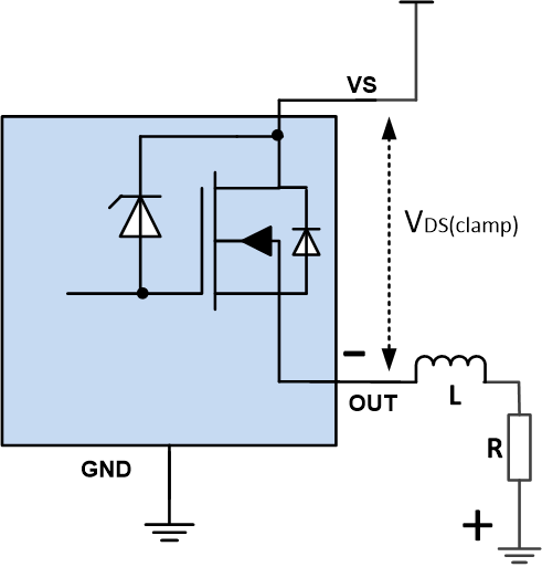
GUID-6E32D488-47D4-484A-9A45-78C946FFE747-low.gifFigure 7-14 Drain-to-Source Clamping Structure
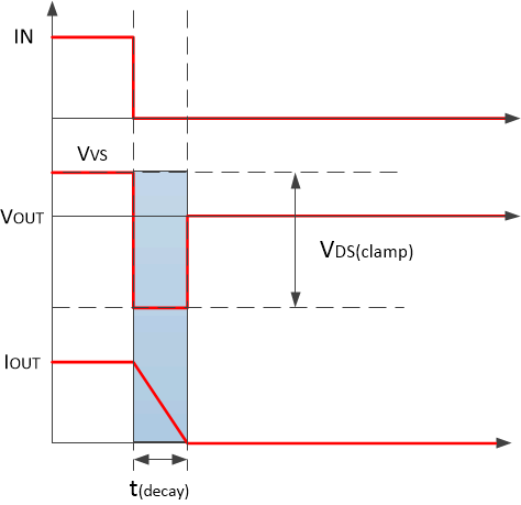
GUID-B09F1265-170B-4EC9-A409-32C4E4F57B84-low.gifFigure 7-15 Inductive-Load Switching-Off Diagram