ZHCSP75A July 2022 – December 2022 TPS1HC30-Q1
PRODUCTION DATA
- 1 特性
- 2 应用
- 3 说明
- 4 Revision History
- 5 Pin Configuration and Functions
- 6 Specifications
- 7 Parameter Measurement Information
-
8 Detailed Description
- 8.1 Overview
- 8.2 Functional Block Diagram
- 8.3
Feature Description
- 8.3.1 Accurate Current Sense
- 8.3.2 Programmable Current Limit
- 8.3.3 Inductive-Load Switching-Off Clamp
- 8.3.4
Full Protections and Diagnostics
- 8.3.4.1 Short-Circuit and Overload Protection
- 8.3.4.2 Open-Load and Short-to-Battery Detection
- 8.3.4.3 Short-to-Battery Detection
- 8.3.4.4 Reverse-Polarity and Battery Protection
- 8.3.4.5 Latch-Off Mode
- 8.3.4.6 Thermal Protection Behavior
- 8.3.4.7 UVLO Protection
- 8.3.4.8 Loss of GND Protection
- 8.3.4.9 Loss of Power Supply Protection
- 8.3.4.10 Reverse Current Protection
- 8.3.4.11 Protection for MCU I/Os
- 8.3.5 Diagnostic Enable Function
- 8.4 Device Functional Modes
- 9 Application and Implementation
- 10Device and Documentation Support
- 11Mechanical, Packaging, and Orderable Information
8.3.1 Accurate Current Sense
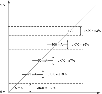
The high-accuracy current-sense function is internally implemented, which allows a better real-time monitoring effect and more-accurate diagnostics without further calibration. A current mirror is used to source 1 / KSNS of the load current, flowing out to the external resistor between the SNS pin and GND, and reflected as voltage on the SNS pin.
KSNS is the ratio of the output current and the sense current. The accuracy values of KSNS quoted in the electrical characteristics do take into consideration temperature and supply voltage. Each device was internally calibrated while in production, so post-calibration by users is not required in most cases.
 Figure 8-1 Current-Sense Accuracy
The maximum voltage out on the SNS pin is clamped to VSNSFH, which is the fault voltage level. To make sure that this voltage is not higher than the system can tolerate, TI has correlated the voltage coming in on the DIAG_EN pin with the maximum voltage out on the SNS pin. If DIAG_EN is between VIH and 3.3 V, the maximum output on the SNS pin is approximately 3.3 V. However, if the voltage at DIAG_EN is above 3.3 V, then the fault SNS voltage, VSNSFH, tracks that voltage up to 5 V. Tracking is done because the GPIO voltage output that is powering the diagnostics through DIAG_EN is close to the maximum acceptable ADC voltage within the same microcontroller. Therefore, the sense resistor value, RSNS, can be chosen to maximize the range of currents needed to be measured by the system. The RSNS value must be chosen based on application need. The maximum usable RSNS value is bounded by the ADC minimum acceptable voltage, VADC,min, for the smallest load current needed to be measured by the system, ILOAD,min. The minimum acceptable RSNS value has to ensure the VSNS voltage is below the VSNSFH value so that the system can determine faults. This difference between the maximum readable current through the SNS pin, ILOAD,max × RSNS, and the VSNSFH is called the headroom voltage, VHR. The headroom voltage is determined by the system but is important so that there is a difference between the maximum readable current and a fault condition. Therefore, the minimum RSNS value has to be the VSNSFH minus the VHR times the sense current ratio, KSNS divided by the maximum load current the system must measure, ILOAD,max. Use the following equation to see the boundary equation.
The maximum current the system wants to read, ILOAD,max, must be below the current-limit threshold because after the current-limit threshold is tripped the VSNS value goes to VSNSFH. Additionally, currents being measured must be below 6 A to ensure that the current sense output is not saturated.
Because this scheme adapts based on the voltage coming in from the MCU, there is no need to have a Zener diode on the SNS pin to protect from high voltages.