SLVSA01C May 2011 – June 2016 TPS2062-Q1 , TPS2065-Q1
PRODUCTION DATA.
- 1 Features
- 2 Applications
- 3 Description
- 4 Revision History
- 5 Pin Configuration and Functions
- 6 Specifications
- 7 Parameter Measurement Information
- 8 Detailed Description
-
9 Application and Implementation
- 9.1
Application Information
- 9.1.1 Overcurrent
- 9.1.2 OC Response
- 9.1.3 Undervoltage Lockout (UVLO)
- 9.1.4 Universal Serial Bus (USB) Applications
- 9.1.5 Host, Self-Powered (SPH), and Bus-Powered Hubs (BPH)
- 9.1.6 Low-Power Bus-Powered and High-Power Bus-Powered Functions
- 9.1.7 USB Power-Distribution Requirements
- 9.1.8 Generic Hot-Plug Applications
- 9.2 Typical Application
- 9.1
Application Information
- 10Power Supply Recommendations
- 11Layout
- 12Device and Documentation Support
- 13Mechanical, Packaging, and Orderable Information
11 Layout
11.1 Layout Guidelines
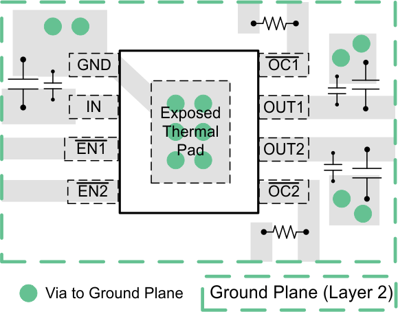
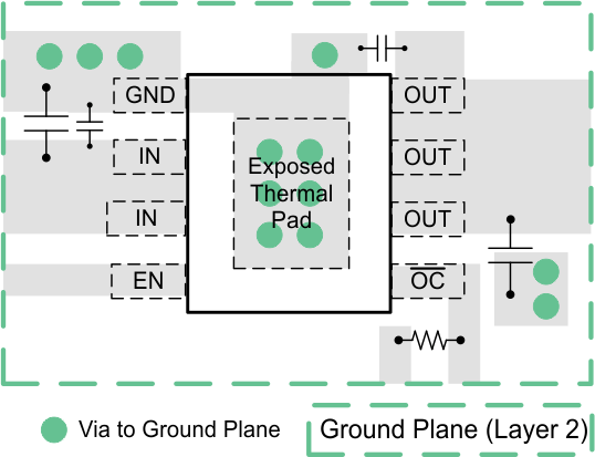
- Place the filter and bypass capacitor between IN and GND as close as possible ensuring a low-impedance trace for IN and a low-impedance trace and via path from GND to ground plane.
- Place the output filter capacitor as close as possible to OUT between OUT and GND. Place the higher-value electrolytic bypass capacitor between OUT and GND. The bypass capacitor is recommended when large transient currents are expected on the output. The OUT trace must be low-impedance to the load.
- Place the pullup resistor for OCx between the pullup voltage source and OCx.
11.2 Layout Examples
 Figure 33. Layout Example for TPS2062-Q1
 Figure 34. Layout Example for TPS2065-Q1
11.3 Thermal Considerations
Thermal protection prevents damage to the IC when heavy-overload or short-circuit faults are present for extended periods of time. The TPS2065-Q1 and TPS2062-Q1 implement a thermal sensing to monitor the operating junction temperature of the power distribution switch. In an overcurrent or short-circuit condition, the junction temperature rises due to excessive power dissipation. Once the die temperature rises above a minimum of 135°C due to overcurrent conditions, the internal thermal-sense circuitry turns the power switch off, thus preventing the power switch from damage. Hysteresis is built into the thermal-sense circuit, and after the device has cooled approximately 10°C, the switch turns back ON. The switch continues to cycle in this manner until the load fault or input power is removed. The OCx open-drain output is asserted (active low, with a 10-ms deglitch) when an overtemperature shutdown or overcurrent occurs.
11.4 Power Dissipation and Junction Temperature
The low ON-resistance on the N-channel MOSFET allows the small surface-mount packages to pass large currents. The thermal resistances of these packages are high compared to those of power packages; it is good design practice to check power dissipation and junction temperature. Begin by determining the rDS(ON) of the N-channel MOSFET relative to the input voltage and operating temperature. As an initial estimate, use the highest operating ambient temperature of interest and read rDS(ON) from Figure 9. Using this value, the power dissipation per switch can be calculated using Equation 1:
Multiply this number by the number of switches being used. This step renders the total power dissipation from the N-channel MOSFETs.
The thermal resistance, RθJA = 1 / (DERATING FACTOR), where DERATING FACTOR is obtained from Dissipation Ratings. Thermal resistance is a strong function of the printed-circuit board construction, and the copper trace area connecting the integrated circuit.
Finally, calculate the junction temperature with Equation 2:
where
- TA= Ambient temperature °C
- RθJA = Thermal resistance
- PD = Total power dissipation based on number of switches being used.
Compare the calculated junction temperature with the initial estimate. If they do not agree within a few degrees, repeat the calculation, using the calculated value as the new estimate. Two or three iterations are generally sufficient to get a reasonable answer.