SLVSA01C May 2011 – June 2016 TPS2062-Q1 , TPS2065-Q1
PRODUCTION DATA.
- 1 Features
- 2 Applications
- 3 Description
- 4 Revision History
- 5 Pin Configuration and Functions
- 6 Specifications
- 7 Parameter Measurement Information
- 8 Detailed Description
-
9 Application and Implementation
- 9.1
Application Information
- 9.1.1 Overcurrent
- 9.1.2 OC Response
- 9.1.3 Undervoltage Lockout (UVLO)
- 9.1.4 Universal Serial Bus (USB) Applications
- 9.1.5 Host, Self-Powered (SPH), and Bus-Powered Hubs (BPH)
- 9.1.6 Low-Power Bus-Powered and High-Power Bus-Powered Functions
- 9.1.7 USB Power-Distribution Requirements
- 9.1.8 Generic Hot-Plug Applications
- 9.2 Typical Application
- 9.1
Application Information
- 10Power Supply Recommendations
- 11Layout
- 12Device and Documentation Support
- 13Mechanical, Packaging, and Orderable Information
7 Parameter Measurement Information
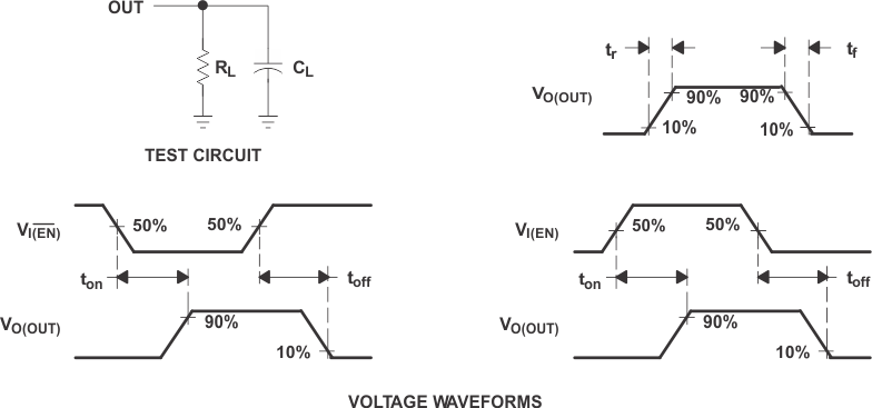 Figure 14. Test Circuit and Voltage Waveforms
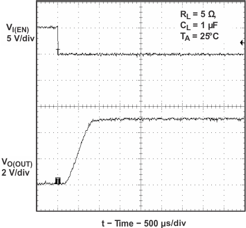 Figure 15. Turnon Delay and Rise Time With 1-μF Load
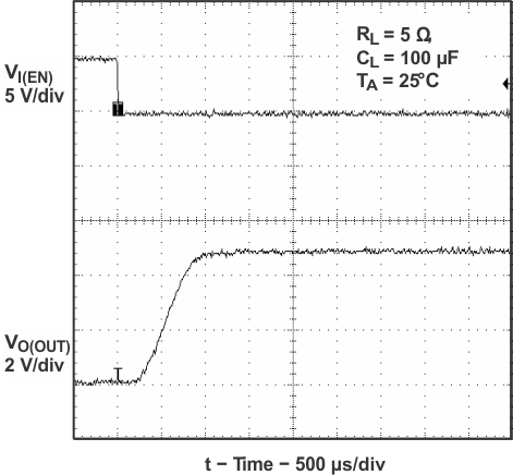 Figure 17. Turnon Delay and Rise Time With 100-μF Load
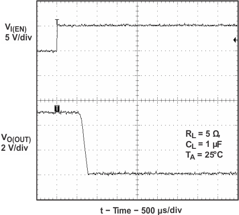 Figure 16. Turnoff Delay and Fall Time With 1-μF Load
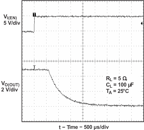 Figure 18. Turnoff Delay and Fall Time With 100-μF Load
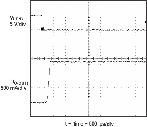 Figure 19. Short-Circuit Current,
Device Enabled Into Short
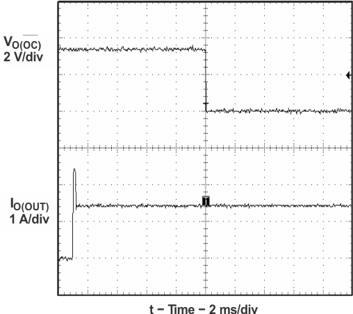 Figure 21. 2-Ω Load Connected to Enabled Device
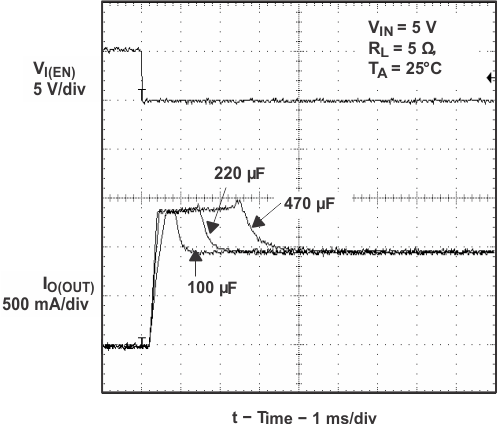 Figure 20. Inrush Current With Different
Load Capacitance
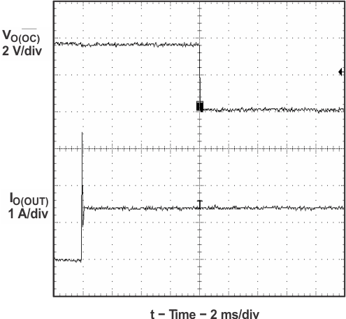 Figure 22. 1-Ω Load Connected to Enabled Device