ZHCSRR9K December 2003 – June 2024 TPS2061 , TPS2062 , TPS2063 , TPS2065 , TPS2066 , TPS2067
PRODUCTION DATA
- 1
- 1 特性
- 2 应用
- 3 说明
- 4 说明(续)
- 5 Pin Configuration and Functions
- 6 Specifications
- 7 Parameter Measurement Information
- 8 Detailed Description
-
9 Application and Implementation
- 9.1
Application Information
- 9.1.1 Power-supply Considerations
- 9.1.2 OC Response
- 9.1.3 Power Dissipation and Junction Temperature
- 9.1.4 Thermal Protection
- 9.1.5 Undervoltage Lockout (UVLO)
- 9.1.6 Universal Serial Bus (USB) Applications
- 9.1.7 Host/Self-Powered and Bus-powered Hubs
- 9.1.8 Low-power Bus-powered and High-Power Bus-Powered Functions
- 9.1.9 USB Power-distribution Requirements
- 9.1.10 Generic Hot-Plug Applications
- 9.1
Application Information
- 10Device and Documentation Support
- 11Revision History
- 12Mechanical, Packaging, and Orderable Information
封装选项
请参考 PDF 数据表获取器件具体的封装图。
机械数据 (封装 | 引脚)
- D|8
- DBV|5
- DGN|8
散热焊盘机械数据 (封装 | 引脚)
- DGN|8
订购信息
9.1.1 Power-supply Considerations
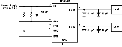
 Figure 9-1 Typical Application
A 0.01-μF to 0.1-μF ceramic bypass capacitor between IN and GND, close to the device, is recommended. Placing a high-value electrolytic capacitor on the output pin(s) is recommended when the output load is heavy. This precaution reduces power-supply transients that may cause ringing on the input. Additionally, bypassing the output with a 0.01-μF to 0.1-μF ceramic capacitor improves the immunity of the device to short-circuit transients.