ZHCSCL6 July 2014 TPS2105-EP
PRODUCTION DATA.
- 1 特性
- 2 应用范围
- 3 说明
- 4 修订历史记录
- 5 Pin Configuration and Functions
- 6 Specifications
- 7 Detailed Description
- 8 Application and Implementation
- 9 Power Supply Recommendations
- 10Layout
- 11器件和文档支持
- 12机械封装和可订购信息
7 Detailed Description
7.1 Overview
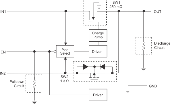
The TPS2105 is a dual-input, single-output power switch designed to provide uninterrupted output voltage when transitioning between two independent power supplies.
The device combines one N-channel (250-m) MOSFET with a single output. The P-channel MOSFET (IN2) is used with auxiliary power supplies that deliver lower current for standby modes. The N-channel MOSFET (IN1) is used with a main power supply that delivers higher current required for normal operation.
The low on-resistance makes the N-channel the ideal path for higher main supply current when power-supply regulation and system voltage drops are critical. When using the P-channel MOSFET, quiescent current is reduced to 0.75 µA to decrease the demand on the standby power supply.
The MOSFETs in the device do not have the parasitic diodes, typically found in discrete MOSFETs, thereby preventing back-flow current when the switch is off.
7.2 Functional Block Diagram

7.3 Feature Description
7.3.1 Power Switches
7.3.1.1 N-Channel MOSFET
The IN1-OUT N-channel MOSFET power switch has a typical on-resistance of 250 mΩ at 5-V input voltage and is configured as a high-side switch.
7.3.1.2 P-Channel MOSFET
The IN2-OUT P-channel MOSFET power switch has a typical on-resistance of 1.3 Ω at 5-V input voltage and is configured as a high-side switch. When operating, the P-channel MOSFET quiescent current is reduced to typically 0.75 µA.
7.3.1.3 Charge Pump
An internal charge pump supplies power to the driver circuit and provides the necessary voltage to pull the gate of the MOSFET above the source. The charge pump operates from input voltages as low as 2.7 V and requires very little supply current.
7.3.1.4 Driver
The driver controls the gate voltage of the IN1-OUT and IN2-OUT power switches. To limit large current surges and reduce the associated electromagnetic interference (EMI) produced, the drivers incorporate circuitry that controls the rise times and fall times of the output voltage.
7.3.1.5 Enable
The logic enable turns on the IN2-OUT power switch when a logic low is present on EN. A logic high on EN restores bias to the drive and control circuits and turns on the IN1-OUT power switch. The enable input is compatible with both TTL and CMOS logic levels.
7.4 Device Functional Modes
7.4.1 Operation With EN Control
The logic enable turns on the IN1-OUT power switch when a logic high is present on EN. Also, a logic low present on EN turns off the IN1-OUT and turns on the IN2-OUT power switch.