ZHCSHY9 April 2018 TPS22810-Q1
PRODUCTION DATA.
8.3.3 EN/UVLO
EN/UVLO controls the ON and OFF state of the internal MOSFET, as an input pin. In its high state, the internal MOSFET is enabled. A low on this pin turns off the internal MOSFET. High and Low levels are specified in the parametric table of the datasheet.
A voltage VEN/UVLO< VENF on this pin turns off the internal FET, thus disconnecting VIN from VOUT, while voltage below VSHUTF takes the device into shutdown mode, with IQ less than 1 μA to ensure minimal power loss.
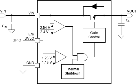
The EN/UVLO pin can be directly driven by a 1.8 V, 3.3 V or 5 V general purpose output pin.
The internal de-glitch delay on EN/UVLO falling edge is intentionally kept low (2.5 μs typical) for quick detection of power failure. For applications where a higher de-glitch delay on EN/UVLO is desired, or when the supply is particularly noisy, it is recommended to use an external bypass capacitor from EN/UVLO to GND.
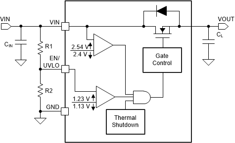
The undervoltage lock out (UVLO) threshold can be programmed by using an external resistor divider from supply VIN terminal to EN/UVLO terminal to GND shown in Figure 18. When an undervoltage or input power fail event is detected, the internal FET is quickly turned off. If the programmable UVLO function is not needed, the EN/UVLO terminal must be connected to the VIN terminal. EN/UVLO terminal must not be left floating.
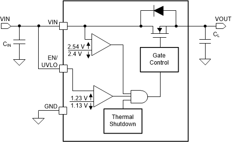
The device also implements internal UVLO circuitry on the VIN terminal. The device disables when the VIN terminal voltage falls below internal UVLO Threshold (VUVF). The internal UVLO threshold has a hysteresis (VUVRhyst). See Figure 19 and Figure 20.
 Figure 18. Configuring UVLO with External Resistor Network
 Figure 19. Using 1.8 V/3.3 V GPIO Signal Directly from Processor
 Figure 20. Default UVLO Threshold VUVR Using No Additional External Components