ZHCSDR1 April 2015 TPS22860
PRODUCTION DATA.
11 Layout
11.1 Layout Guidelines
For best operational performance of the device, use good PCB layout practices, including:
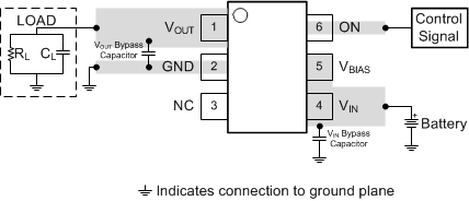
- VIN and VOUT traces should be as short and wide as possible to accommodate for high current.
- The VIN pin should be bypassed to ground with low ESR ceramic bypass capacitors. The typical recommended bypass capacitance is 1-μF ceramic with X5R or X7R dielectric. This capacitor should be placed as close to the device pins as possible.
- The VOUT pin should be bypassed to ground with low ESR ceramic bypass capacitors. The typical recommended bypass capacitance is one-tenth of the VIN bypass capacitor of X5R or X7R dielectric rating. This capacitor should be placed as close to the device pins as possible.
11.2 Thermal Reliability
For higher reliability it is recommended to limit TPS22860 IC’s die junction temperature to less than 105°C. The IC junction temperature is directly proportional to the on-chip power dissipation. Use the following equation to calculate maximum on-chip power dissipation to achieve the maximum die junction temperature target:

11.3 Improving Package Thermal Performance
The package RθJA value under standard conditions on a High-K board is listed in the Thermal Information table. RθJA value depends on the PC board layout. An external heat sink and/or a cooling mechanism, like a cold air fan, can help reduce RθJA and thus improve device thermal capabilities. Refer to TI’s design support web page at www.ti.com/thermal for a general guidance on improving device thermal performance.
11.4 Layout Example
 Figure 11. Basic PCB Layout