ZHCSF76B July   2016  – December 2019 TPS22918-Q1

PRODUCTION DATA.  

  1. 特性
  2. 应用
  3. 说明
    1.     Device Images
      1.      简化原理图
      2.      导通电阻与输入电压间的关系典型值
  4. 修订历史记录
  5. Pin Configuration and Functions
    1.     Pin Functions
  6. Specifications
    1. 6.1 Absolute Maximum Ratings
    2. 6.2 ESD Ratings
    3. 6.3 Recommended Operating Conditions
    4. 6.4 Thermal Information
    5. 6.5 Electrical Characteristics
    6. 6.6 Switching Characteristics
    7. 6.7 Typical DC Characteristics
    8. 6.8 Typical AC Characteristics
  7. Parameter Measurement Information
  8. Detailed Description
    1. 8.1 Overview
    2. 8.2 Functional Block Diagram
    3. 8.3 Feature Description
      1. 8.3.1 On and Off Control
      2. 8.3.2 Quick Output Discharge (QOD)
        1. 8.3.2.1 QOD when System Power is Removed
        2. 8.3.2.2 Internal QOD Considerations
      3. 8.3.3 Adjustable Rise Time (CT)
    4. 8.4 Device Functional Modes
  9. Application and Implementation
    1. 9.1 Application Information
    2. 9.2 Typical Application
      1. 9.2.1 Design Requirements
      2. 9.2.2 Detailed Design Procedure
        1. 9.2.2.1 Input Capacitor (CIN)
        2. 9.2.2.2 Output Capacitor (CL) (Optional)
        3. 9.2.2.3 Shutdown Sequencing During Unexpected System Power Loss
        4. 9.2.2.4 VIN to VOUT Voltage Drop
        5. 9.2.2.5 Inrush Current
      3. 9.2.3 Application Curves
  10. 10Power Supply Recommendations
  11. 11Layout
    1. 11.1 Layout Guidelines
    2. 11.2 Layout Example
    3. 11.3 Thermal Considerations
  12. 12器件和文档支持
    1. 12.1 器件支持
      1. 12.1.1 开发支持
    2. 12.2 文档支持
      1. 12.2.1 相关文档
    3. 12.3 接收文档更新通知
    4. 12.4 社区资源
    5. 12.5 商标
    6. 12.6 静电放电警告
    7. 12.7 Glossary
  13. 13机械、封装和可订购信息

封装选项

机械数据 (封装 | 引脚)
散热焊盘机械数据 (封装 | 引脚)
订购信息

Shutdown Sequencing During Unexpected System Power Loss

Microcontrollers and processors often have a specific shutdown sequence in which power must be removed. Using the adjustable Quick Output Discharge function of the TPS22918-Q1, adding a load switch to each power rail can be used to manage the power down sequencing in the event of an unexpected system power loss (battery removal). To determine the QOD values for each load switch, first confirm the power down order of the device this is wished to power sequence. Be sure to check if there are voltage or timing margins that must be maintained during power down. Next, refer to Table 1 in the Quick Output Discharge (QOD) section to determine appropriate COUT and RQOD values for each power rail's load switch so that the load switches' fall times correspond to the order in which they need to be powered down. In the above example, make sure this power rail's fall time to be 4 ms. Using Equation 2, to determine the appropriate RQOD to achieve our desired fall time.
Because fall times are measured from 90% of VOUT to 10% of VOUT, Equation 2 becomes Equation 4.

Equation 4. .5 V = 4.5 V × e-(4 ms) / (R × (22 µF))
Equation 5. RQOD = 83.333 Ω

Refer to Figure 7, RPD at VIN = 5 V is approximately 25 Ω. Using Equation 1, the required external QOD resistance can be calculated as shown in Equation 6.

Equation 6. 83.333 Ω = 25 Ω + REXT
Equation 7. REXT = 58.333 Ω

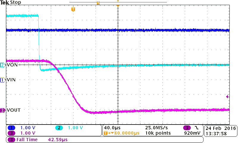
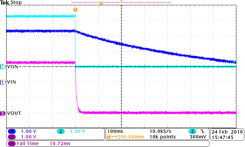
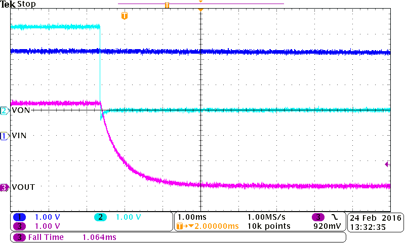
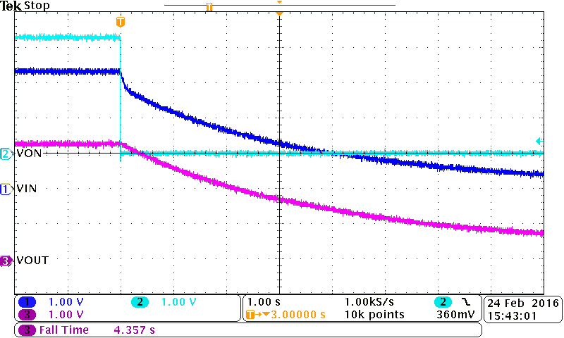
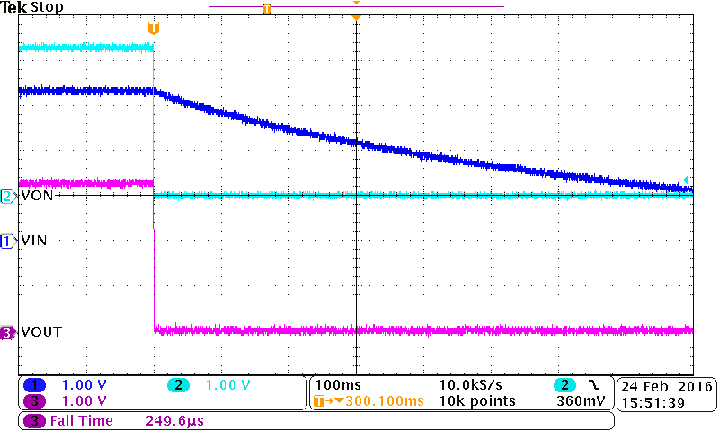
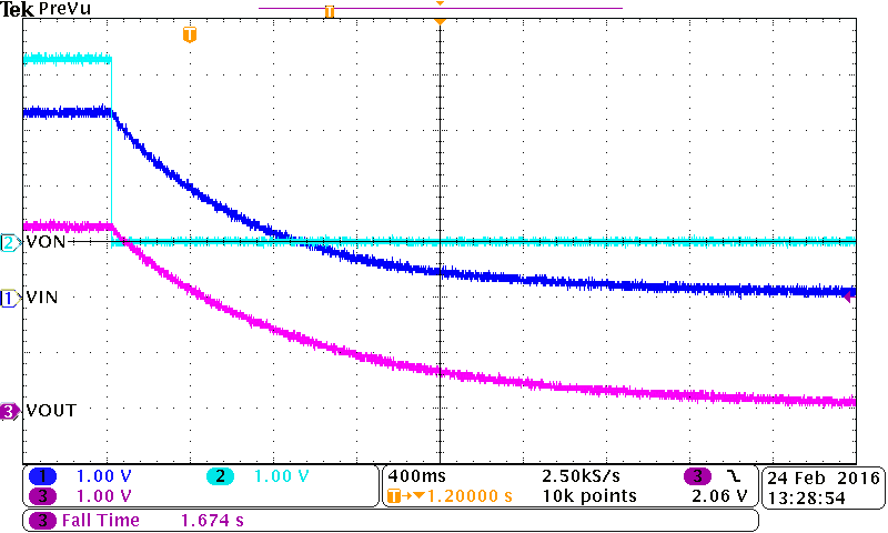
Figure 24 through Figure 29 are scope shots demonstrating an example of the QOD functionality when power is removed from the device (both ON and VIN are disconnected simultaneously). The input voltage is decaying in all scope shots below.

  • Initial VIN = 3.3 V
  • QOD = Open, 500 Ω, or shorted to VOUT
  • CL = 1 μF, 10 μF
  • VOUT is left floating

NOTE: VIN may appear constant in some figures. This is because the time scale of the scope shot is too small to show the decay of CIN.
TPS22918-Q1 tFall with QOD_CIN=COUT=1uF_VIN=3.3V_QOD=Open.png
VIN = 3.3 V CIN = 1 µF CL = 1 µF
QOD = Open
Figure 24. Fall Time (tF) at VIN = 3.3 V
TPS22918-Q1 tFall with QOD_CIN=COUT=1uF_VIN=3.3V_QOD=VOUT.png
VIN = 3.3 V CIN = 1 µF CL = 1 µF
QOD = VOUT
Figure 26. Fall Time (tF) at VIN = 3.3 V
TPS22918-Q1 tFall with QOD_CIN=COUT=10uF_VIN=3.3V_QOD=500ohm_zommed out.png
VIN = 3.3 V CIN = 1 µF CL = 10 µF
QOD = 500 Ω
Figure 28. Fall Time (tF) at VIN = 3.3 V
TPS22918-Q1 tFall with QOD_CIN=COUT=1uF_VIN=3.3V_QOD=500ohm.png
VIN = 3.3 V CIN = 1 µF CL = 1 µF
QOD = 500 Ω
Figure 25. Fall Time (tF) at VIN = 3.3 V
TPS22918-Q1 tFall with QOD_CIN=COUT=10uF_VIN=3.3V_QOD=Open.png
VIN = 3.3 V CIN = 1 µF CL = 10 µF
QOD = Open
Figure 27. Fall Time (tF) at VIN = 3.3 V
TPS22918-Q1 tFall with QOD_CIN=COUT=10uF_VIN=3.3V_QOD=VOUT_zoomed out.png
VIN = 3.3 V CIN = 1 µF CL = 10 µF
QOD = VOUT
Figure 29. Fall Time (tF) at VIN = 3.3 V