SLVS832D November   2008  – July 2014 TPS22941 , TPS22942 , TPS22943 , TPS22944 , TPS22945

PRODUCTION DATA.  

  1. Features
  2. Applications
  3. Description
  4. Revision History
  5. Device Comparison Table
  6. Pin Configuration and Functions
  7. Specifications
    1. 7.1 Absolute Maximum Ratings
    2. 7.2 Handling Ratings
    3. 7.3 Recommended Operating Conditions
    4. 7.4 Thermal Information
    5. 7.5 Electrical Characteristics
    6. 7.6 Switching Characteristics
    7. 7.7 Typical Characteristics
  8. Detailed Description
    1. 8.1 Overview
    2. 8.2 Functional Block Diagram
    3. 8.3 Feature Description
      1. 8.3.1 Fault Reporting
      2. 8.3.2 Current Limiting
      3. 8.3.3 Thermal Shutdown
    4. 8.4 Device Functional Modes
  9. Application and Implementation
    1. 9.1 Application Information
      1. 9.1.1 On/Off Control
      2. 9.1.2 Undervoltage Lockout
      3. 9.1.3 Reverse Voltage
      4. 9.1.4 Input Capacitor
      5. 9.1.5 Output Capacitor
    2. 9.2 Typical Application
      1. 9.2.1 Design Requirements
      2. 9.2.2 Detailed Design Procedure
        1. 9.2.2.1 VIN to VOUT Voltage Drop
        2. 9.2.2.2 Maximum Output Capacitance
        3. 9.2.2.3 Power Dissipation
        4. 9.2.2.4 Application Curves
  10. 10Power Supply Recommendations
  11. 11Layout
    1. 11.1 Layout Guidelines
    2. 11.2 Layout Example
    3. 11.3 Thermal Considerations
  12. 12Device and Documentation Support
    1. 12.1 Related Links
    2. 12.2 Trademarks
    3. 12.3 Electrostatic Discharge Caution
    4. 12.4 Glossary
  13. 13Mechanical, Packaging, and Orderable Information

封装选项

机械数据 (封装 | 引脚)
散热焊盘机械数据 (封装 | 引脚)
订购信息

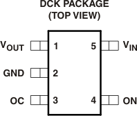
6 Pin Configuration and Functions

po1_lvs832.gif

Pin Functions

PIN TYPE DESCRIPTION
NAME SOT (DCK)
PIN NO.
VOUT 1 O Switch Output. Place ceramic bypass capacitor(s) between this terminal and GND. See the Application Information section for more information.
GND 2 Ground
OC 3 O Over current output flag: active LOW, open drain output that indicates an over current, supply under voltage, or over temperature state.
ON 4 I Switch control input. Do not leave floating.
VIN 5 I Switch Input. Place ceramic bypass capacitor(s) between this terminal and GND. See the Application Information section for more information.