ZHCSDK9A March 2015 – April 2015 TPS22953 , TPS22954
PRODUCTION DATA.
- 1 特性
- 2 应用
- 3 说明
- 4 简化电路原理图
- 5 修订历史记录
- 6 Device Comparison Table
- 7 Pin Configuration and Functions
-
8 Specifications
- 8.1 Absolute Maximum Ratings
- 8.2 ESD Ratings
- 8.3 Recommended Operating Conditions
- 8.4 Thermal Information
- 8.5 Electrical Characteristics
- 8.6 Electrical Characteristics, VBIAS = 5 V
- 8.7 Electrical Characteristics, VBIAS = 3.3 V
- 8.8 Electrical Characteristics, VBIAS = 2.5 V
- 8.9 Switching Characteristics, CT = 1000 pF
- 8.10 Switching Characteristics, CT = 0 pF
- 8.11 Typical DC Characteristics
- 8.12 Typical Switching Characteristics
-
9 Detailed Description
- 9.1 Overview
- 9.2 Functional Block Diagram
- 9.3
Feature Description
- 9.3.1 On/Off Control (EN pin)
- 9.3.2 Voltage Monitoring (SNS pin)
- 9.3.3 Power Good (PG Pin)
- 9.3.4 Supervisor Fault Detection and Automatic Restart
- 9.3.5 Manual Restart
- 9.3.6 Thermal Shutdown
- 9.3.7 Quick Output Discharge (QOD) (TPS22954 Only)
- 9.3.8 VIN and VBIAS Voltage Range
- 9.3.9 Adjustable Rise Time (CT pin)
- 9.4 Device Functional Modes
- 10Application and Implementation
- 11Power Supply Recommendations
- 12Layout
- 13器件和文档支持
- 14机械封装和可订购信息
封装选项
机械数据 (封装 | 引脚)
散热焊盘机械数据 (封装 | 引脚)
- DQC|10
订购信息
9 Detailed Description
9.1 Overview
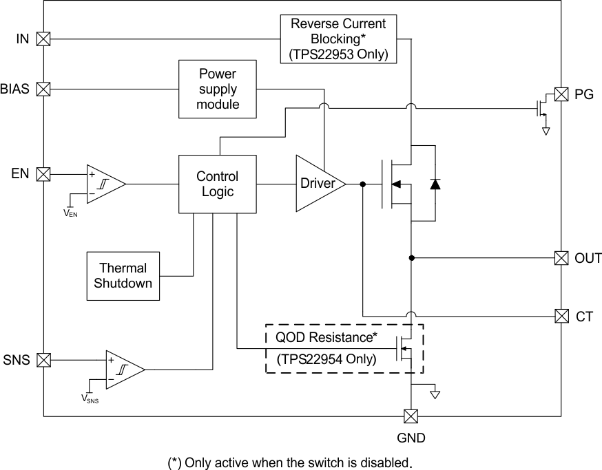
The TPS22953/4 are 5.7-V, 5-A load switches in 10-pin SON packages. To reduce voltage drop for low voltage, high current rails the device implements a low resistance N-channel MOSFET, which reduces the drop out voltage through the device at high currents. The integrated adjustable undervoltage lockout (UVLO) and adjustable power good (PG) threshold provides voltage monitoring as well as robust power sequencing.
The adjustable rise time control of the device greatly reduces inrush current for a wide variety of bulk load capacitances, thereby reducing or eliminating power supply droop. The switch is independently controlled by an on/off input (EN), which is capable of interfacing directly with low-voltage control signals. A 15 Ω on-chip load resistor is integrated into the device for output quick discharge when switch is turned off.
During shutdown, the device has very low leakage currents, thereby reducing unneccessary leakages for downstream modules during standby. Integrated power monitoring functionality, control logic, driver, power supply, and output discharge FET eliminates the need for any external components, which reduces solution size and BOM count.
9.2 Functional Block Diagram
9.3 Feature Description
9.3.1 On/Off Control (EN pin)
The EN pin controls the state of the switch. When the voltage on EN has exceeded VIH,EN the switch will be enabled. When EN goes below VIL,EN the switch is disabled.
The EN pin has a blanking time of tBLANK on the rising edge once the VIH,EN threshold has been exceeded. It also has a deglitch time of tDEGLITCH when the voltage has gone below VIL,EN.
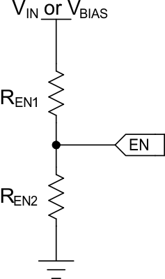
The EN pin can also be configured via an external resistor divider to monitor a voltage signal for input UVLO. Refer to the equation and diagram below on how to configure the EN pin for input UVLO.

Where:
VIH,EN = the rising threshold of the EN pin (see Electrical Characteristics table)
VIN = the input voltage being monitored (this could be VIN, VBIAS, or an external power supply)
REN1, REN2 = resistor divider values
9.3.2 Voltage Monitoring (SNS pin)
The SNS pin of the device can be used to monitor the output voltage of the device or another voltage rail. The pin can be configured with an external resistor divider to set the desired trip point for the voltage being monitored or be tied to OUT directly. If the voltage on the SNS pin exceeds VIH,SNS, the voltage being monitored on the SNS pin is considered to be valid high. The voltage on the SNS pin must be greater than VIH,SNS for at least tBLANK before PG is asserted high. If the voltage on the SNS pin goes below VIL,SNS, then the switch will power cycle (i.e., the switch will be disabled and re-enabled). For proper functionality of the device, this pin must not be left floating. If a resistor divider is not being used for voltage sensing, this pin can be tied directly to VOUT.
The SNS pin has a blanking time of tBLANK on the rising edge once the VIH,SNS threshold has been exceeded. It has a deglitch time of tDEGLITCH when the voltage has gone below VIL,SNS.
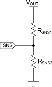
Refer to the equation and diagram below on how to configure the SNS pin for voltage monitoring.

Where:
VIH,SNS = the rising threshold of the SNS pin (see Electrical Characteristics table)
VOUT = voltage on the OUTpin
RSNS1, RSNS2 = resistor divider values
9.3.3 Power Good (PG Pin)
The PG pin is only asserted high when the voltage on EN has exceeded VIH,EN and the voltage on SNS has exceeded VIH,SNS. There is a tBLANK time, typically 100µs, between the SNS voltage exceeding VIH,SNS and PG being asserted high. If the voltage on EN goes below VIL,EN or the voltage on SNS goes below VIL,SNS, PG will be de-asserted. There is a tDEGLITCH time, typically 5µs, between the EN voltage or SNS voltage going below their respective VIL levels and PG being pulled low.
PG is an open drain pin and must be pulled up with a pull-up resistor. Be sure to never exceed the maximum operating voltage on this pin. If PG is not being used in the application, tie it to GND for proper device functionality.
For proper PG operation, the BIAS voltage should be within the recommended operating range. In systems that are very sensitive to noise or have long PG traces, it is recommended to add a small capacitance from PG to GND to for decoupling.
9.3.4 Supervisor Fault Detection and Automatic Restart
The falling edge of the SNS pin below VIL,SNS is considered a fault case and will cause the load switch to be disabled for tRESTART (typically 2ms). After the tRESTART time, the switch will be automatically re-enabled as long as EN is still above VIH,EN . In the case the SNS pin is being used to monitor VOUT or a downstream voltage, the restart will help to protect against excessive over-current if there is a quick short to GND.
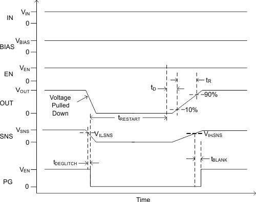 Figure 50. Automatic Restart after Quick Short to GND
9.3.5 Manual Restart
The falling edge of the SNS pin below VIL,SNS is considered a fault case and will cause the load switch to be disabled for tRESTART (typically 2ms). The SNS pin can be driven by an MCU to manually reset the load switch. After the tRESTART time, the switch will be automatically re-enabled as long as EN is still above VIH,EN , even is SNS is held low. The PG pin will stay low until the switch is re-enabled and the SNS pin rises above VIH,SNS.
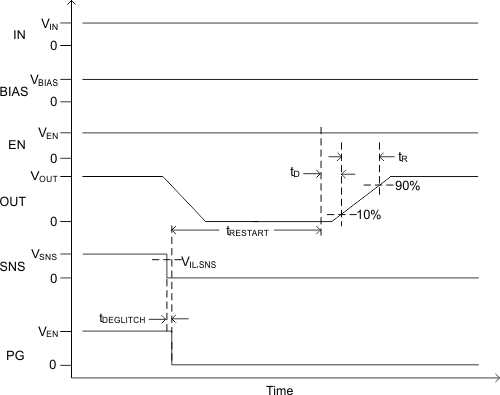 Figure 51. Manual Restart (SNS Held Low)
If the SNS pin is brought above VIH,SNS within the tRESTART time, the switch will still wait to re-enable. The PG pin will also stay low until tBLANK after switch is re-enabled. In this case, PG will indicate when the switch is enabled and capable of being reset again.
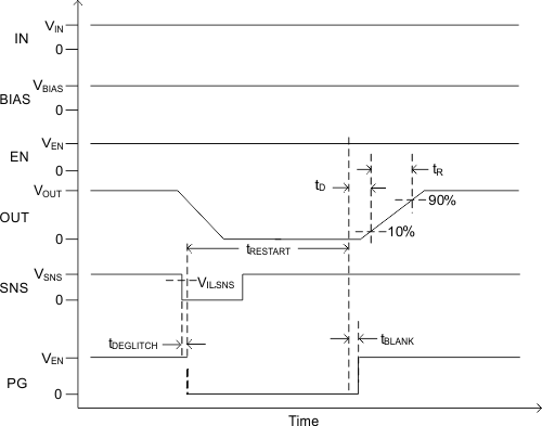 Figure 52. Manual Restart (SNS Toggled Low to High)
9.3.6 Thermal Shutdown
If the junction temperature of the device exceeds TSD, the switch will be disabled. The device will be enabled once the junction temperature drops by TSDHYS as long as EN is still greater than VIH,EN.
9.3.7 Quick Output Discharge (QOD) (TPS22954 Only)
The quick output discharge (QOD) transistor is engaged indefinitely whenever the switch is disabled and the recommended VBIAS voltage is met. During this state, the QOD resistance (RPD) will discharge VOUT to GND. It is not recommended to apply a continuous DC voltage to OUT when the device is disabled.
The QOD transistor can remain active for a short period of time even after VBIAS looses power. This brief period of time is defined as tDIS. For best results, it is recommended the device get disabled before VBIAS goes below the minimum recommended voltage. The waveform below shows the behaviour when power is applied and then removed in a typical application.
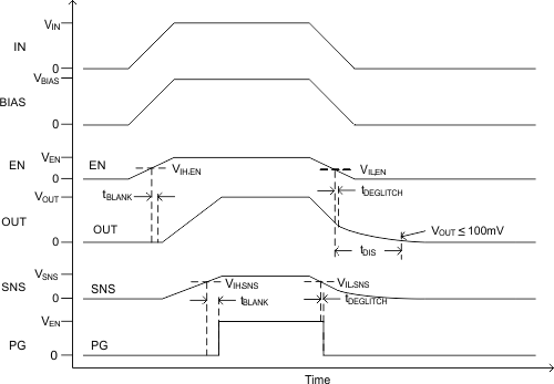 Figure 53. Power Applied and then Removed in a Typical Application
At the end of the tDIS time, it is not guaranteed that VOUT will be 0V since the final voltage will be dependent upon the initial voltage and the CL capacitor. The final VOUT can be calculated with the following formula for a given initial voltage and CL capacitor.

Where:
Vf = final VOUT voltage
Vo = initial VOUT voltage
R = the value of the output discharge resistor, RPD (see Electrical Characteristics table)
C = the output bulk capacitance on OUT
9.3.8 VIN and VBIAS Voltage Range
For optimal RON performance, make sure VIN ≤ VBIAS. The device will still be functional if VIN > VBIAS but it will exhibit RON greater than what is listed in the Electrical Characteristics table. See Figure 50 for an example of a typical device. Notice the increasing RON as VIN increases. Be sure to never exceed the maximum voltage rating for VIN and VBIAS.
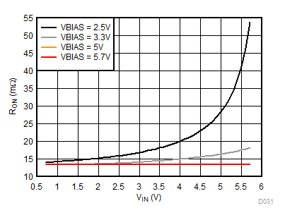 Figure 54. RON When VIN > VBIAS
9.3.9 Adjustable Rise Time (CT pin)
A capacitor to GND on the CT pin sets the slew rate for VOUT. An appropriate capacitance value should be placed on CT such that the IMAX and IPLS specifications of the device are not violated. The capacitor to GND on the CT pin should be rated for 25 V or higher. An approximate formula for the relationship between CT (except for CT = open) and the slew rate for any VBIAS is:
where
- SR = slew rate (in μs/V)
- CT = the capacitance value on the CT terminal (in pF)
- The units for the constant 20 are μs/V.
- The units for the constant 0.35 are μs/(V*pF).
Rise time can be calculated by multiplying the input voltage (typically 10% to 90%) by the slew rate. The table below contains rise time values measured on a typical device.
| CTx (pF) | RISE TIME (µs) 10%–90%, CL = 0.1 µF, VBIAS = 2.5V to 5.7V, RL=10Ω LOAD. TYPICAL VALUES AT 25°C, 25V X7R 10% CERAMIC CAP |
|||||
|---|---|---|---|---|---|---|
| 5V | 3.3V | 1.8V | 1.5V | 1.2V | 0.7V | |
| Open | 140 | 98 | 62 | 54 | 46 | 32 |
| 220 | 444 | 301 | 175 | 150 | 124 | 81 |
| 470 | 767 | 518 | 299 | 255 | 210 | 133 |
| 1000 | 1492 | 994 | 562 | 474 | 387 | 245 |
| 2200 | 3105 | 2050 | 1151 | 961 | 787 | 490 |
| 4700 | 6420 | 4246 | 2365 | 1980 | 1612 | 998 |
| 10000 | 14059 | 9339 | 5183 | 4331 | 3533 | 2197 |
9.4 Device Functional Modes
The following Table describes what the OUT pin will be connected to for a particular device as determined by the EN pin.
| EN | TPS22953 | TPS22954 |
|---|---|---|
| L | OPEN | RPD to GND |
| H | IN | IN |