ZHCSCK3A June   2014  – June 2014 TPS22959

PRODUCTION DATA.  

  1. 特性
  2. 应用范围
  3. 说明
  4. 简化电路原理图
  5. 修订历史记录
  6. Pin Configuration and Functions
  7. Specifications
    1. 7.1 Absolute Maximum Ratings
    2. 7.2 Handling Ratings
    3. 7.3 Recommended Operating Conditions
    4. 7.4 Thermal Information
    5. 7.5 Electrical Characteristics, VBIAS = 5.0 V
    6. 7.6 Electrical Characteristics, VBIAS = 2.5 V
    7. 7.7 Switching Characteristics
    8. 7.8 Typical Characteristics
  8. Detailed Description
    1. 8.1 Overview
    2. 8.2 Functional Block Diagram
    3. 8.3 Feature Description
      1. 8.3.1 On/off Control
      2. 8.3.2 Input Capacitor (CIN)
      3. 8.3.3 Output Capacitor (CL)
      4. 8.3.4 VIN and VBIAS Voltage Range
    4. 8.4 Device Functional Modes
  9. Applications and Implementation
    1. 9.1 Application Information
    2. 9.2 Typical Application
      1. 9.2.1 Design Requirements
      2. 9.2.2 Detailed Design Procedure
        1. 9.2.2.1 VIN to VOUT Voltage Drop
        2. 9.2.2.2 Inrush Current
        3. 9.2.2.3 Thermal Considerations
      3. 9.2.3 Application Curves
  10. 10Power Supply Recommendations
  11. 11Layout
    1. 11.1 Layout Guidelines
    2. 11.2 Layout Example
  12. 12器件和文档支持
    1. 12.1 商标
    2. 12.2 静电放电警告
    3. 12.3 术语表
  13. 13机械封装和可订购信息

封装选项

机械数据 (封装 | 引脚)
散热焊盘机械数据 (封装 | 引脚)
订购信息

11 Layout

11.1 Layout Guidelines

  • VIN and VOUT traces should be as short and wide as possible to accommodate for high current.
  • Use vias under the exposed thermal pad for thermal relief for high current operation.
  • The VIN pin should be bypassed to ground with low ESR ceramic bypass capacitors. The typical recommended bypass capacitance is 1-µF ceramic with X5R or X7R dielectric. This capacitor should be placed as close to the device pins as possible.
  • The VOUT pin should be bypassed to ground with low ESR ceramic bypass capacitors. The typical recommended bypass capacitance is one-tenth of the VIN bypass capacitor of X5R or X7R dielectric rating. This capacitor should be placed as close to the device pins as possible.
  • The VBIAS pin should be bypassed to ground with low ESR ceramic bypass capacitors. The typical recommended bypass capacitance is 0.1-µF ceramic with X5R or X7R dielectric.

11.2 Layout Example
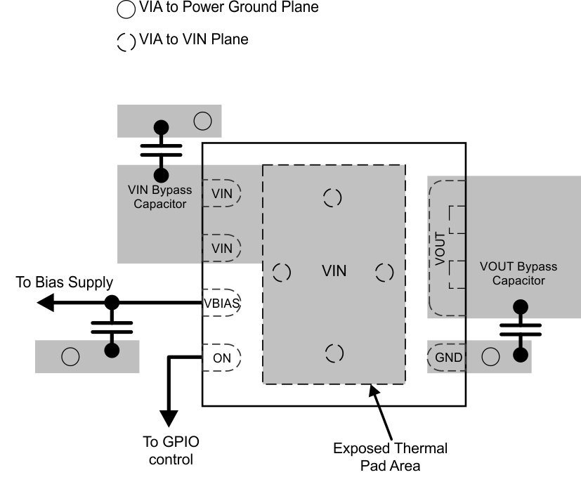
rec_bd_lay_slvsci4.gifFigure 42. Recommended Board Layout