TPS22965 5.7V,6A,16mΩ 导通电阻负载开关
1 特性
- 集成单通道负载开关
- 输入电压范围:0.8V 至 5.7V
- 超低导通电阻 (RON)
- V输入 = 5V(V偏置 = 5V)时,R导通 = 16mΩ
- V输入 = 3.6V(V偏置 = 5V)时,R导通 = 16mΩ
- V输入 = 1.8V(V偏置 = 5V)时,R导通 = 16mΩ
- 6A 最大持续开关电流
- 低静态电流 (50µA)
- 低控制输入阀值支持使用
1.2V,1.8V,2.5V 和 3.3V 逻辑电路 - 可配置的上升时间
- 快速输出放电 (QOD)
- 带有散热垫的小外形尺寸无引线 (SON) 8 引脚封装
- 根据 JESD 22 测试得出的静电放电 (ESD) 性能
- 2000V 人体模型 (HBM) 和 1000V 充电器件模型 (CDM)
2 应用范围
- Ultrabook™
- 笔记本电脑/上网本
- 平板电脑
- 消费类电子米6体育平台手机版_好二三四
- 机顶盒/家庭网关
- 电信系统
- 固态硬盘 (SSD)
3 说明
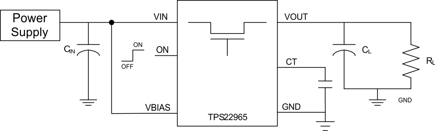
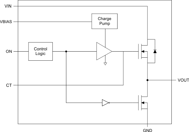
TPS22965 是一款单通道负载开关,可提供可配置的上升时间来尽量减小浪涌电流。 此器件包括一个 N 通道金属氧化物半导体场效应晶体管 (MOSFET),可在 0.8V 至 5.7V 的输入电压范围内运行并可支持 6A 的最大持续电流。此开关由一个开/关输入 (ON) 控制,此输入能够直接连接低电压控制信号。 在 TPS22965 中,为了实现开关关闭时的快速输出放电,增加了一个 225Ω 的片上负载电阻器。
TPS22965 采用小型,节省空间的 2.00mm x 2.00mm 8 引脚 SON 封装 (DSG),且带有集成散热焊盘,支持较高功耗。 器件在自然通风环境下的额定运行温度范围为 -40°C 至 85°C。
器件信息(1)
| 部件号 | 封装 | 封装尺寸(标称值) |
|---|---|---|
| TPS22965 | DSG (8) | 2.00mm x 2.00mm |
- 要了解所有可用封装,请见数据表末尾的可订购米6体育平台手机版_好二三四附录。
4 简化电路原理图
5 修订历史记录
Changes from A Revision (August 2013) to B Revision
- Changed 已将此数据表更改为新的模板布局。Go
- 添加了器件信息表。 Go
- Added Handling Ratings table. Go
- Changed MAX value of "VIN" from 5.5 V to 5.7 V. Go
- Changed MAX value of "VBIAS" from 5.5 V to 5.7 V. Go
- Changed MAX value of "VON" from 5.5 V to 5.7 V.Go
- Added Thermal Information table. Go
- Added Detailed Description Section. Go
- Added Application and Implementation section. Go
- Added Power Supply Recommendations section. Go
- Added Layout section. Go
Changes from * Revision (August 2012) to A Revision
- Updated VON MAX value to fix typo that restricted operating range. Changed MAX value from "VIN" to "5.5" to align with rest of document. Go
6 Pin Configuration and Functions
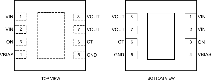
Pin Functions
| PIN | I/O | DESCRIPTION | |
|---|---|---|---|
| NAME | DSG | ||
| CT | 6 | O | Switch slew rate control. Can be left floating. See Application Information section for more information. |
| GND | 5 | – | Device ground. |
| ON | 3 | I | Active high switch control input. Do not leave floating. |
| Thermal Pad | – | – | Thermal pad (exposed center pad) to alleviate thermal stress. Tie to GND. See Layout Example section for layout guidelines. |
| VBIAS | 4 | I | Bias voltage. Power supply to the device. Recommended voltage range for this pin is 2.5V to 5.7V. See Application and Implementation section for more information. |
| VIN | 1, 2 | I | Switch input. Input bypass capacitor recommended for minimizing VIN dip. Must be connected to Pin 1 and Pin 2. See Application and Implementation section for more information. |
| VOUT | 7, 8 | O | Switch output. |
7 Specifications
7.1 Absolute Maximum Ratings
over operating free-air temperature range (unless otherwise noted)(1)(2)| MIN | MAX | UNIT | |||
|---|---|---|---|---|---|
| VIN | Input voltage range | –0.3 | 6 | V | |
| VOUT | Output voltage range | –0.3 | 6 | V | |
| VBIAS | Bias voltage range | –0.3 | 6 | V | |
| VON | Input voltage range | –0.3 | 6 | V | |
| IMAX | Maximum continuous switch current | 6 | A | ||
| IPLS | Maximum pulsed switch current, pulse <300 µs, 2% duty cycle | 8 | A | ||
| TJ | Maximum junction temperature | 125 | °C | ||
7.2 Handling Ratings
| MIN | MAX | UNIT | |||
|---|---|---|---|---|---|
| Tstg | Storage temperature range | –65 | 150 | °C | |
| V(ESD) | Electrostatic discharge | Human body model (HBM), per ANSI/ESDA/JEDEC JS-001, all pins(1) | –2000 | 2000 | V |
| Charged device model (CDM), per JEDEC specification JESD22-C101, all pins(2) | –1000 | 1000 | |||
7.3 Recommended Operating Conditions
| MIN | MAX | UNIT | |||
|---|---|---|---|---|---|
| VIN | Input voltage range | 0.8 | VBIAS | V | |
| VBIAS | Bias voltage range | 2.5 | 5.7 | V | |
| VON | ON voltage range | 0 | 5.7 | V | |
| VOUT | Output voltage range | VIN | V | ||
| VIH | High-level input voltage, ON | VBIAS = 2.5 V to 5.7 V | 1.2 | 5.7 | V |
| VIL | Low-level input voltage, ON | VBIAS = 2.5 V to 5.7 V | 0 | 0.5 | V |
| CIN | Input capacitor | 1(2) | µF | ||
| TA | Operating free-air temperature range(1) | –40 | 85 | °C | |
7.4 Thermal Information
| THERMAL METRIC(1) | TPS22965 | UNIT | |
|---|---|---|---|
| DSG (8 PINS) | |||
| RθJA | Junction-to-ambient thermal resistance | 65.3 | °C/W |
| RθJC(top) | Junction-to-case (top) thermal resistance | 74.2 | |
| RθJB | Junction-to-board thermal resistance | 35.4 | |
| ψJT | Junction-to-top characterization parameter | 2.2 | |
| ψJB | Junction-to-board characterization parameter | 36.0 | |
| RθJC(bot) | Junction-to-case (bottom) thermal resistance | 12.8 | |
7.5 Electrical Characteristics, VBIAS = 5.0 V
Unless otherwise noted, the specification in the following table applies over the operating ambient temperature –40 °C ≤ TA ≤ 85 °C (Full) and VBIAS = 5.0 V. Typical values are for TA = 25 °C.| PARAMETER | TEST CONDITIONS | TA | MIN | TYP | MAX | UNIT | ||
|---|---|---|---|---|---|---|---|---|
| POWER SUPPLIES AND CURRENTS | ||||||||
| IIN(VBIAS-ON) | VBIAS quiescent current | IOUT = 0 mA, VIN = VON = VBIAS = 5.0 V |
Full | 50 | 75 | µA | ||
| IIN(VBIAS-OFF) | VBIAS shutdown current | VON = GND, VOUT = 0 V | Full | 2 | µA | |||
| IIN(VIN-OFF) | VIN off-state supply current | VON = GND, VOUT = 0 V |
VIN = 5.0 V | Full | 0.2 | 8 | µA | |
| VIN = 3.3 V | 0.02 | 3 | ||||||
| VIN = 1.8 V | 0.01 | 2 | ||||||
| VIN = 0.8 V | 0.005 | 1 | ||||||
| ION | ON pin input leakage current | VON = 5.5 V | Full | 0.5 | µA | |||
| RESISTANCE CHARACTERISTICS | ||||||||
| RON | ON-state resistance | IOUT = –200 mA, VBIAS = 5.0 V |
VIN = 5.0 V | 25°C | 16 | 23 | mΩ | |
| Full | 25 | |||||||
| VIN = 3.3 V | 25°C | 16 | 23 | mΩ | ||||
| Full | 25 | |||||||
| VIN = 1.8 V | 25°C | 16 | 23 | mΩ | ||||
| Full | 25 | |||||||
| VIN = 1.5 V | 25°C | 16 | 23 | mΩ | ||||
| Full | 25 | |||||||
| VIN = 1.2 V | 25°C | 16 | 23 | mΩ | ||||
| Full | 25 | |||||||
| VIN = 0.8 V | 25°C | 16 | 23 | mΩ | ||||
| Full | 25 | |||||||
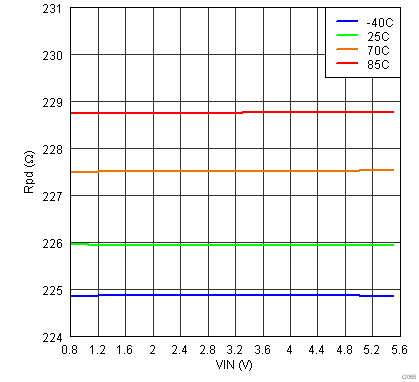
| RPD | Output pull-down resistance | VIN = 5.0 V, VON = 0 V, IOUT = 15 mA | Full | 225 | 300 | Ω | ||
7.6 Electrical Characteristics, VBIAS = 2.5 V
Unless otherwise noted, the specification in the following table applies over the operating ambient temperature –40 °C ≤ TA ≤ 85 °C (Full) and VBIAS = 2.5 V. Typical values are for TA = 25 °C.| PARAMETER | TEST CONDITIONS | TA | MIN | TYP | MAX | UNIT | ||
|---|---|---|---|---|---|---|---|---|
| POWER SUPPLIES AND CURRENTS | ||||||||
| IIN(VBIAS-ON) | VBIAS quiescent current | IOUT = 0 mA, VIN = VON = VBIAS = 2.5 V |
Full | 20 | 30 | µA | ||
| IIN(VBIAS-OFF) | VBIAS shutdown current | VON = GND, VOUT = 0 V | Full | 2 | µA | |||
| IIN(VIN-OFF) | VIN off-state supply current | VON = GND, VOUT = 0 V |
VIN = 2.5 V | Full | 0.01 | 3 | µA | |
| VIN = 1.8 V | 0.01 | 2 | ||||||
| VIN = 1.2 V | 0.005 | 2 | ||||||
| VIN = 0.8 V | 0.003 | 1 | ||||||
| ION | ON pin input leakage current | VON = 5.5 V | Full | 0.5 | µA | |||
| RESISTANCE CHARACTERISTICS | ||||||||
| RON | ON-state resistance | IOUT = –200 mA, VBIAS = 2.5 V |
VIN = 2.5 V | 25°C | 20 | 26 | mΩ | |
| Full | 28 | |||||||
| VIN = 1.8 V | 25°C | 19 | 26 | mΩ | ||||
| Full | 28 | |||||||
| VIN = 1.5 V | 25°C | 18 | 25 | mΩ | ||||
| Full | 27 | |||||||
| VIN = 1.2 V | 25°C | 18 | 25 | mΩ | ||||
| Full | 27 | |||||||
| VIN = 0.8 V | 25°C | 17 | 25 | mΩ | ||||
| Full | 27 | |||||||
| RPD | Output pull-down resistance | VIN = 2.5 V, VON = 0 V, IOUT = 1 mA | Full | 275 | 325 | Ω | ||
7.7 Switching Characteristics
| PARAMETER | TEST CONDITION | MIN | TYP | MAX | UNIT | |
|---|---|---|---|---|---|---|
| VIN = VON = VBIAS = 5 V, TA = 25ºC (unless otherwise noted) | ||||||
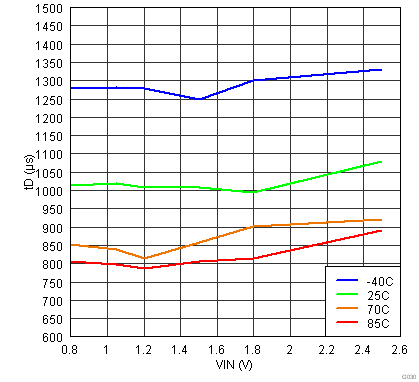
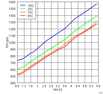
| tON | Turn-on time | RL = 10 Ω, CL = 0.1 µF, CT = 1000 pF | 1325 | µs | ||
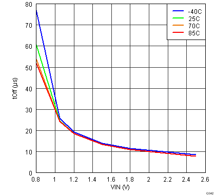
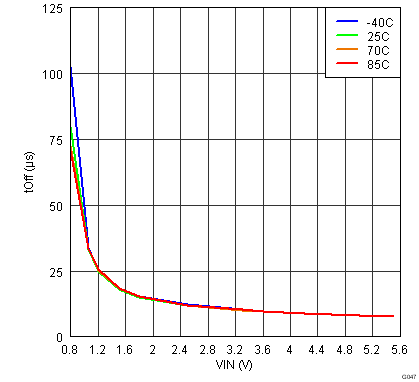
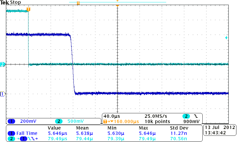
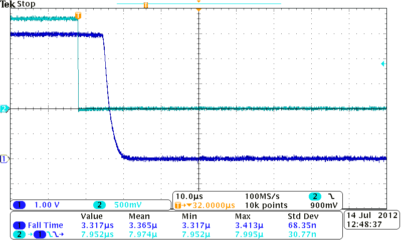
| tOFF | Turn-off time | 10 | ||||
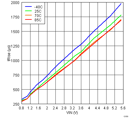
| tR | VOUT rise time | 1625 | ||||
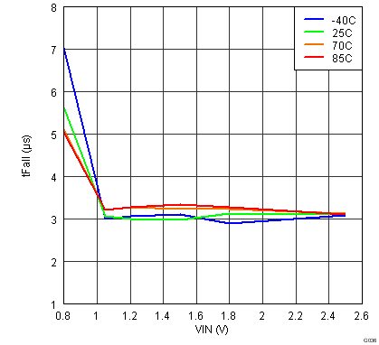
| tF | VOUT fall time | 3.5 | ||||
| tD | ON delay time | 500 | ||||
| VIN = 0.8 V, VON = VBIAS = 5 V, TA = 25ºC (unless otherwise noted) | ||||||
| tON | Turn-on time | RL = 10 Ω, CL = 0.1 µF, CT = 1000 pF | 600 | µs | ||
| tOFF | Turn-off time | 80 | ||||
| tR | VOUT rise time | 300 | ||||
| tF | VOUT fall time | 5.5 | ||||
| tD | ON delay time | 460 | ||||
| VIN = 2.5V, VON = 5 V, VBIAS = 2.5 V, TA = 25ºC (unless otherwise noted) | ||||||
| tON | Turn-on time | RL = 10 Ω, CL = 0.1 µF, CT = 1000 pF | 2200 | µs | ||
| tOFF | Turn-off time | 9 | ||||
| tR | VOUT rise time | 2275 | ||||
| tF | VOUT fall time | 3.1 | ||||
| tD | ON delay time | 1075 | ||||
| VIN = 0.8 V, VON = 5 V, VBIAS = 2.5 V, TA = 25ºC (unless otherwise noted) | ||||||
| tON | Turn-on time | RL = 10 Ω, CL = 0.1 µF, CT = 1000 pF | 1450 | µs | ||
| tOFF | Turn-off time | 60 | ||||
| tR | VOUT rise time | 875 | ||||
| tF | VOUT fall time | 5.5 | ||||
| tD | ON delay time | 1010 | ||||
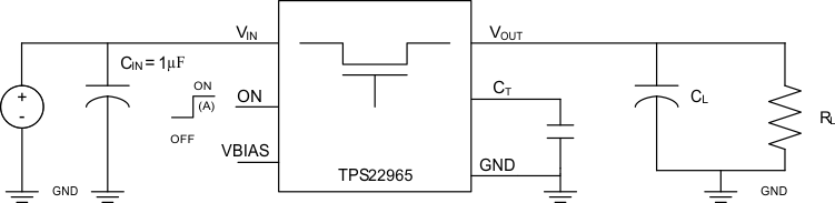
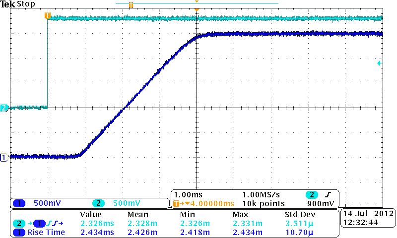
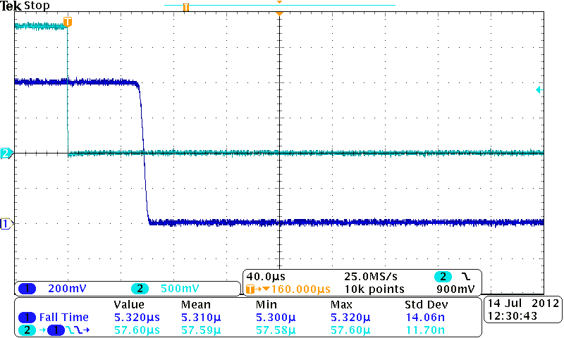
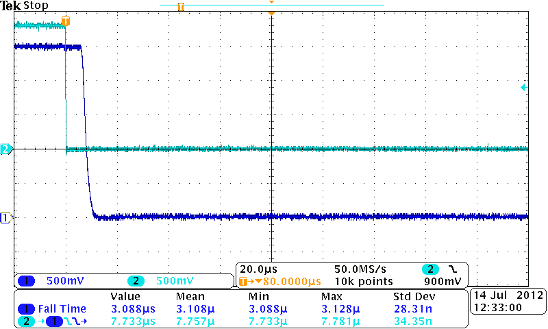
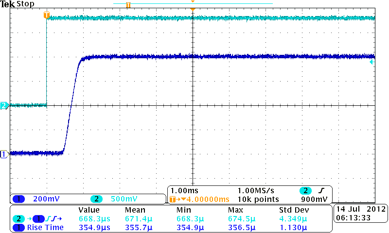
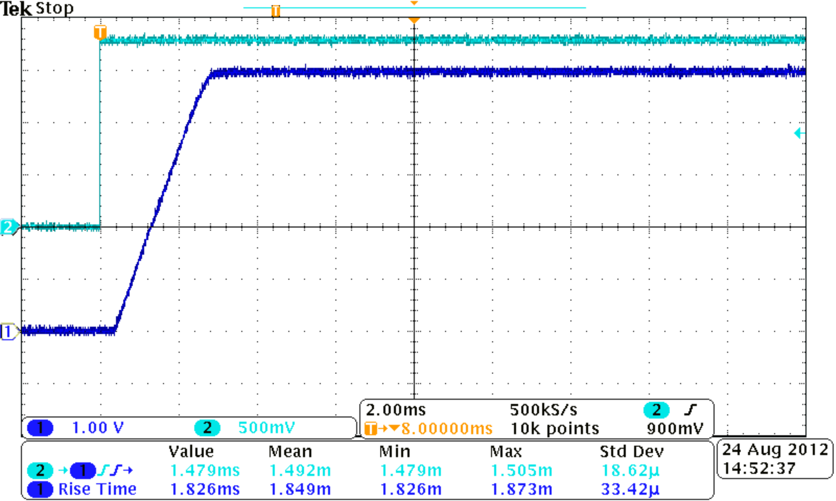
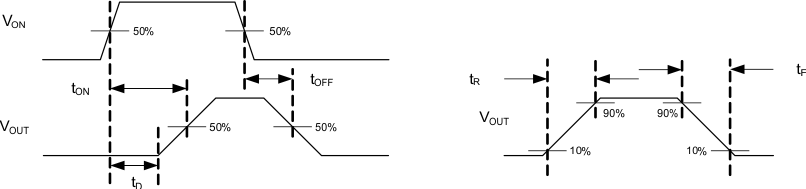 Figure 2. tON/tOFF Waveforms
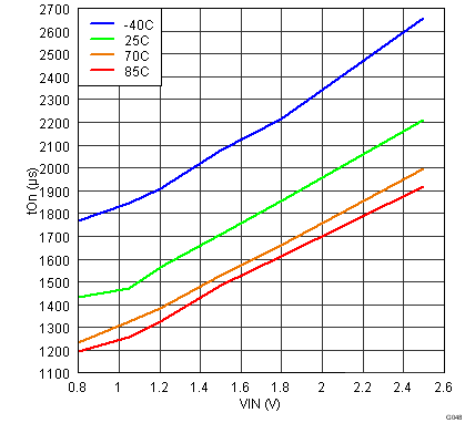
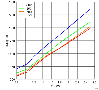
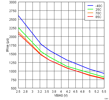
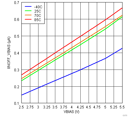
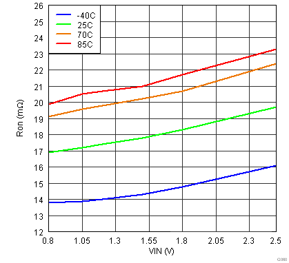
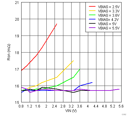
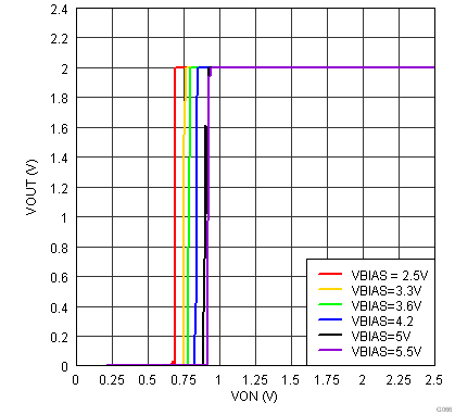
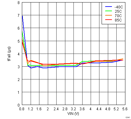
7.8 Typical Characteristics
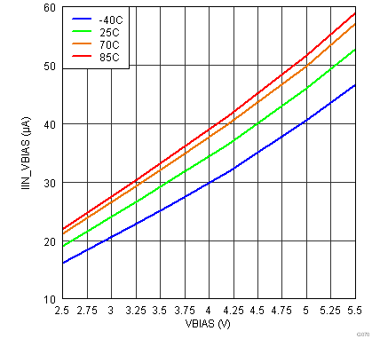
| VIN = VBIAS | VON = 5 V | VOUT = Open |
| VBIAS = 5.5 V | VON = 0 V | VOUT = 0 V |
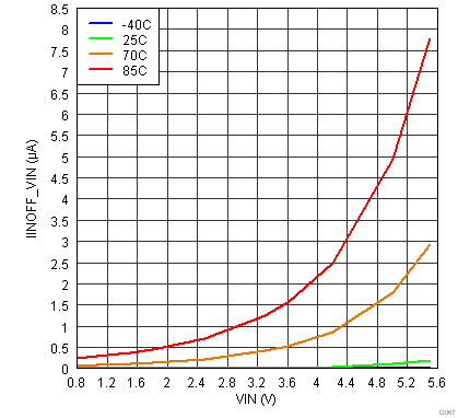
| VBIAS = 5.5 V | IOUT = –200 mA |
| VBIAS = 5.5 V | IOUT = –200 mA |
| VBIAS = 5.5 V | VON = 0 V | IPD = 1 mA |
| VBIAS = 2.5 V | CT = 1 nF |
| VBIAS = 2.5 V | CT = 1 nF |
| VBIAS = 2.5 V | CT = 1 nF |
| VBIAS = 2.5 V | CT = 1 nF |
| VBIAS = 2.5 V | CT = 1 nF |
| VIN = 2.5 V | CT = 1 nF |
| VIN = VBIAS | VON = 0 V | VOUT = 0 V |

| VBIAS = 2.5 V | IOUT = –200 mA |
| VBIAS = 2.5 V | IOUT = –200 mA |
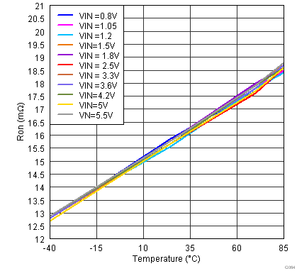
| TA = 25 °C | IOUT = –200 mA |
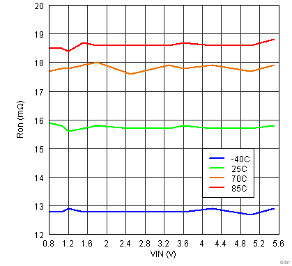
| TA = 25 °C | VIN = 2 V |

| VBIAS = 5.5 V | CT = 1 nF |
| VBIAS = 5.5 V | CT = 1 nF |
| VBIAS = 5.5 V | CT = 1 nF |
| VBIAS = 5.5 V | CT = 1 nF |
| VBIAS = 5.5 V | CT = 1 nF |
7.9 Typical Switching Characteristics
TA = 25 °C, CT = 1 nF, CIN = 1 µF, CL = 0.1 µF, RL = 10 Ω, CH1 = VOUT, CH2 = VON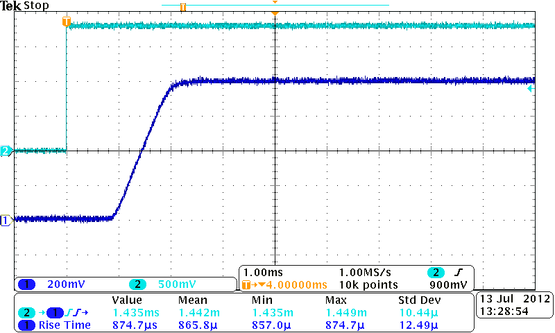
| VIN = 0.8 V | VBIAS = 2.5 V | CIN = 1 µF |
| CL = 0.1 µF | RL = 10 Ω |
| VIN = 2.5 V | VBIAS = 2.5 V | CIN = 1 µF, |
| CL = 0.1 µF | RL = 10 Ω |
| VIN = 0.8 V | VBIAS = 2.5 V | CIN = 1 µF |
| CL = 0.1 µF | RL = 10 Ω |
| VIN = 2.5 V | VBIAS = 2.5 V | CIN = 1 µF |
| CL = 0.1 µF | RL = 10 Ω |
| VIN = 0.8 V | VBIAS = 5.0 V | CIN = 1 µF |
| CL = 0.1 µF | RL = 10 Ω |
| VIN = 5.0 V | VBIAS = 5.0 V | CIN = 1 µF |
| CL = 0.1 µF | RL = 10 Ω |
| VIN = 0.8 V | VBIAS = 5.0 V | CIN = 1 µF |
| CL = 0.1 µF | RL = 10 Ω |
| VIN = 5.0 V | VBIAS = 5.0 V | CIN = 1 µF |
| CL = 0.1 µF | RL = 10 Ω) |
8 Detailed Description
8.1 Overview
The device is a single channel, 6-A load switch in an 8-terminal SON package. To reduce the voltage drop in high current rails, the device implements an ultra-low resistance N-channel MOSFET. The device has a programmable slew rate for applications that require specific rise-time.
The device has very low leakage current during off state. This prevents downstream circuits from pulling high standby current from the supply. Integrated control logic, driver, power supply, and output discharge FET eliminates the need for any external components, which reduces solution size and bill of materials (BOM) count.
8.2 Functional Block Diagram
8.3 Feature Description
8.3.1 Adjustable Rise Time
A capacitor to GND on the CT terminal sets the slew rate. The voltage on the CT terminal can be as high as 12 V. Therefore, the minimum voltage rating for the CT cap should be 25 V for optimal performance. An approximate formula for the relationship between CT and slew rate when VBIAS is set to 5 V is shown in Equation 1 below. This equation accounts for 10% to 90% measurement on VOUT and does NOT apply for CT = 0 pF. Use table below to determine rise times for when CT = 0 pF.

Where,
SR = slew rate (in µs/V)
CT = the capacitance value on the CT terminal (in pF)
The units for the constant 13.4 are µs/V. The units for the constant 0.39 are µs/(V*pF).
Rise time can be calculated by multiplying the input voltage by the slew rate. The table below contains rise time values measured on a typical device. Rise times shown below are only valid for the power-up sequence where VIN and VBIAS are already in steady state condition before the ON terminal is asserted high.
Table 1. Rise Time vs CT Capacitor
| CT (pF) | RISE TIME (µs) 10% - 90%, CL = 0.1 µF, CIN = 1 µF, RL = 10 Ω, VBIAS = 5 V TYPICAL VALUES at 25°C with a 25V X7R 10% CERAMIC CAPACITOR on CT |
||||||
|---|---|---|---|---|---|---|---|
| VIN = 5 V | VIN = 3.3 V | VIN = 1.8 V | VIN = 1.5 V | VIN = 1.2 V | VIN = 1.05 V | VIN = 0.8 V | |
| 0 | 127 | 93 | 62 | 55 | 51 | 46 | 42 |
| 220 | 475 | 314 | 188 | 162 | 141 | 125 | 103 |
| 470 | 939 | 637 | 359 | 304 | 255 | 218 | 188 |
| 1000 | 1869 | 1229 | 684 | 567 | 476 | 414 | 344 |
| 2200 | 4020 | 2614 | 1469 | 1211 | 1024 | 876 | 681 |
| 4700 | 8690 | 5746 | 3167 | 2703 | 2139 | 1877 | 1568 |
| 10000 | 18360 | 12550 | 6849 | 5836 | 4782 | 4089 | 3449 |
8.3.2 Quick Output Discharge
The TPS22965 includes a Quick Output Discharge (QOD) feature. When the switch is disabled, a discharge resistor is connected between VOUT and GND. This resistor has a typical value of 225-Ω and prevents the output from floating while the switch is disabled.
8.3.3 Low Power Consumption During Off State
The ISD VIN supply current is 0.01-µA typical at 1.8-VIN. Typically, the downstream loads would have a significantly higher off-state leakage current. The load switch allows system standby power consumption to be reduced.
8.4 Device Functional Modes
Table 2. Functional Table
| ON | VIN to VOUT | VOUT to GND |
|---|---|---|
| L | Off | On |
| H | On | Off |