ZHCSA62B August   2012  – August 2014 TPS22965

PRODUCTION DATA.  

  1. 特性
  2. 应用范围
  3. 说明
  4. 简化电路原理图
  5. 修订历史记录
  6. Pin Configuration and Functions
  7. Specifications
    1. 7.1 Absolute Maximum Ratings
    2. 7.2 Handling Ratings
    3. 7.3 Recommended Operating Conditions
    4. 7.4 Thermal Information
    5. 7.5 Electrical Characteristics, VBIAS = 5.0 V
    6. 7.6 Electrical Characteristics, VBIAS = 2.5 V
    7. 7.7 Switching Characteristics
    8. 7.8 Typical Characteristics
    9. 7.9 Typical Switching Characteristics
  8. Detailed Description
    1. 8.1 Overview
    2. 8.2 Functional Block Diagram
    3. 8.3 Feature Description
      1. 8.3.1 Adjustable Rise Time
      2. 8.3.2 Quick Output Discharge
      3. 8.3.3 Low Power Consumption During Off State
    4. 8.4 Device Functional Modes
  9. Application and Implementation
    1. 9.1 Application Information
      1. 9.1.1 ON/OFF Control
      2. 9.1.2 Input Capacitor (Optional)
      3. 9.1.3 Output Capacitor (Optional)
      4. 9.1.4 VIN and VBIAS Voltage Range
    2. 9.2 Typical Application
      1. 9.2.1 Design Requirements
      2. 9.2.2 Detailed Design Procedure
        1. 9.2.2.1 Inrush Current
      3. 9.2.3 Application Curves
  10. 10Power Supply Recommendations
  11. 11Layout
    1. 11.1 Layout Guidelines
    2. 11.2 Layout Example
    3. 11.3 Thermal Considerations
  12. 12器件和文档支持
    1. 12.1 商标
    2. 12.2 静电放电警告
    3. 12.3 术语表
  13. 13机械封装和可订购信息

封装选项

机械数据 (封装 | 引脚)
散热焊盘机械数据 (封装 | 引脚)
订购信息

11 Layout

11.1 Layout Guidelines

For best performance, all traces should be as short as possible. To be most effective, the input and output capacitors should be placed close to the device to minimize the effects that parasitic trace inductances may have on normal operation. Using wide traces for VIN, VOUT, and GND helps minimize the parasitic electrical effects along with minimizing the case to ambient thermal impedance. The CT trace should be as short as possible to avoid parasitic capacitance.

11.2 Layout Example
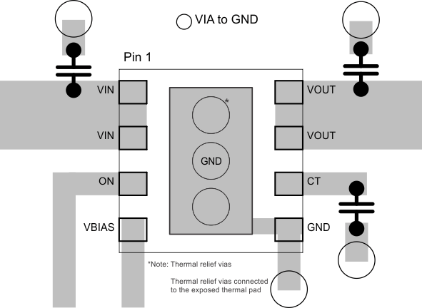
lay_exp_slvsci3.gif

11.3 Thermal Considerations

The maximum IC junction temperature should be restricted to 125°C under normal operating conditions. To calculate the maximum allowable dissipation, PD(max) for a given output current and ambient temperature, use the following equation as a guideline:

Equation 5. eq2_lvsbh4.gif

Where:

PD(max) = maximum allowable power dissipation
TJ(max) = maximum allowable junction temperature (125°C for the TPS22965)
TA = ambient temperature of the device
ΘJA = junction to air thermal impedance. See Thermal Information section. This parameter is highly dependent upon board layout.

Refer to the Layout Example, notice that the thermal vias are located under the exposed thermal pad of the device. This allows for thermal diffusion away from the device.