SLVSBH4F June 2012 – July 2016 TPS22966
PRODUCTION DATA.
- 1 Features
- 2 Applications
- 3 Description
- 4 Revision History
- 5 Pin Configuration and Functions
- 6 Specifications
- 7 Parameter Measurement Information
- 8 Detailed Description
- 9 Application and Implementation
- 10Power Supply Recommendations
- 11Layout
- 12Device and Documentation Support
- 13Mechanical, Packaging, and Orderable Information
1 Features
- Input Voltage Range: 0.8 V to 5.5 V
- Integrated Dual-Channel Load Switch
- On-Resistance
- RON = 16 mΩ at VIN = 5 V (VBIAS = 5 V)
- RON = 16 mΩ at VIN = 3.6 V (VBIAS = 5 V)
- RON = 16 mΩ at VIN = 1.8 V (VBIAS = 5 V)
- 6-A Maximum Continuous Switch Current per Channel
- Low Quiescent Current
- 80 µA (Both Channels)
- 60 µA (Single Channel)
- Low Control Input Threshold Enables Use of
1.2-, 1.8-, 2.5-, and 3.3-V Logic - Configurable Rise Time
- Quick Output Discharge (QOD) (Optional)
- SON 14-Pin Package With Thermal Pad
- ESD Performance Tested per JESD 22
- 2-kV HBM and 1-kV CDM
2 Applications
- Ultrabook™
- Notebooks and Netbooks
- Tablet PCs
- Consumer Electronics
- Set-top Boxes and Residental Gateways
- Telecom Systems
- Solid-State Drives (SSD)
3 Description
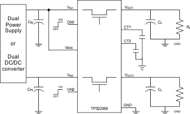
The TPS22966 is a small, low RON, dual-channel load switch with controlled turnon. The device contains two N-channel MOSFETs that can operate over an input voltage range of 0.8 V to 5.5 V and can support a maximum continuous current of 6 A per channel. Each switch is independently controlled by an on and off input (ON1 and ON2), which can interface directly with low-voltage control signals. In TPS22966, a 220-Ω on-chip load resistor is added for quick-output discharge when switch is turned off.
The TPS22966 is available in a small, space-saving 2-mm × 3-mm 14-SON package (DPU) with integrated thermal pad allowing for high power dissipation. The device is characterized for operation over the free-air temperature range of –40°C to +105°C.
Device Information(1)
| PART NUMBER | PACKAGE | BODY SIZE (NOM) |
|---|---|---|
| TPS22966 | WSON (14) | 3.00 mm × 2.00 mm |
- For all available packages, see the orderable addendum at the end of the data sheet.
