ZHCSCN4F January 2014 – July 2017 TPS22968
PRODUCTION DATA.
- 1 特性
- 2 应用
- 3 说明
- 4 修订历史记录
- 5 Device Comparison
- 6 Pin Configuration and Functions
- 7 Specifications
- 8 Parameter Measurement Information
- 9 Detailed Description
- 10Application and Implementation
- 11Power Supply Recommendations
- 12Layout
- 13器件和文档支持
- 14机械、封装和可订购信息
9 Detailed Description
9.1 Overview
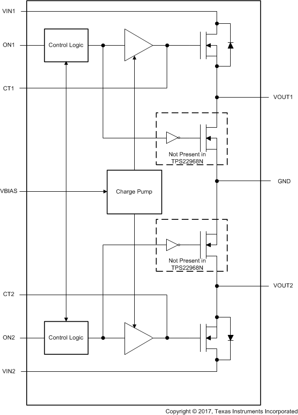
The TPS22968 is a 5.5-V, 4-A, dual-channel ultra-low RON load switch with controlled turnon. The device contains two N-channel MOSFETs. Each channel can support a maximum continuous current of 4 A and is controlled by an on and off GPIO-compatible input. The ON pin must be connected and cannot be left floating. The device is designed to control the turnon rate and therefore the inrush current. By controlling the inrush current, power supply sag can be reduced during turnon. The slew rate for each channel is set by connecting a capacitor to GND on the CT pins.
The slew rate is proportional to the capacitor on the CT pin. See the Adjustable Rise Time section to determine the correct CT value for a desired rise time.
The internal circuitry is powered by the VBIAS pin, which supports voltages from 2.5 V to 5.5 V. This circuitry includes the charge pump, QOD (optional), and control logic. For these internal blocks to function correctly, a voltage between 2.5 V and 5.5 V must be supplied to VBIAS.
When a voltage is supplied to VBIAS, the ON1 pin goes low, and the ON2 pins go low, the QOD turns on. This connects VOUT1 and VOUT2 to GND through an on-chip resistor. The typical pulldown resistance (RPD) is
270 Ω.
9.2 Functional Block Diagram

9.3 Feature Description
9.3.1 ON and OFF Control
The ON pins control the state of the switch. Asserting ON high enables the switch. ON is active high and has a low threshold, making it capable of interfacing with low-voltage signals. The ON pin is compatible with standard GPIO logic threshold. It can be used with any microcontroller with 1.2 V or higher GPIO voltage. This pin cannot be left floating and must be tied either high or low for proper functionality.
9.3.2 Input Capacitor (Optional)
When the switch turns on into a discharged load capacitor or short-circuit, a capacitor must be placed between VIN and GND to limit the voltage drop on the input supply caused by transient inrush currents. A 1-µF ceramic capacitor (CIN), placed close to the pins, is sufficient. Higher values of CIN can be used to further reduce the voltage drop during high-current application. When switching heavy loads, TI recommends having an input capacitor 10x higher than the output capacitor to avoid excessive voltage drop.
9.3.3 Output Capacitor (Optional)
TI highly recommends a CIN greater than CL, because of the integrated body diode in the NMOS switch. A CL greater than CIN can cause the voltage on VOUT to exceed VIN when the system supply is removed. This could result in current flow through the body diode from VOUT to VIN. TI recommends a CIN to CL ratio of 10 to 1 for minimizing VIN dip caused by inrush currents during startup.
9.3.4 QOD (Optional)
The TPS22968 includes a QOD feature. When the switch is disabled, a discharge resistor is connected between VOUT and GND. This resistor has a typical value of 270 Ω and prevents the output from floating while the switch is disabled.
9.3.5 VIN and VBIAS Voltage Range
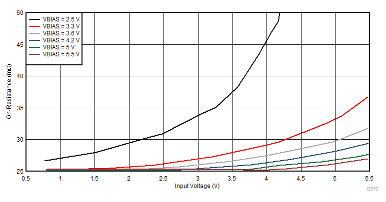
For optimal RON performance, make sure VIN ≤ VBIAS. The device is still functional if VIN > VBIAS, but it exhibits RON greater than what is listed in the Electrical Characteristics (VBIAS = 5 V) and Electrical Characteristics (VBIAS = 2.5 V) table. See Figure 30 for an example of a typical device. Notice the increasing RON as VIN exceeds VBIAS voltage. Be sure to never exceed the maximum voltage rating for VIN and VBIAS.

| Temperature = 25°C | IOUT = 200 mA | |||
9.3.6 Adjustable Rise Time
A capacitor to GND on the CT pins sets the slew rate for each channel. The capacitor to GND on the CT pins must be rated for 25 V and above. An approximate formula for the relationship between CT and slew rate with VBIAS = 5 V is shown in Equation 1.
where
- SR is the slew rate (in µs/V)
- CT is the capacitance value on the CT pin (in pF)
- The units for the constant 13.7 is in µs/V.
Rise time can be calculated by multiplying the input voltage by the slew rate. Table 1 contains rise time values measured on a typical device.
Table 1. Rise Time Table
| CTx (pF) | Typical values at 25°C with a 25-V X7R 10% ceramic capacitor on CT (1) | ||||||
|---|---|---|---|---|---|---|---|
| VIN = 5 V | VIN = 3.3 V | VIN = 2.5 V | VIN = 1.8 V | VIN = 1.5 V | VIN = 1.2V | VIN = 0.8 V | |
| 0 | 65 | 48 | 41 | 35 | 31 | 29 | 24 |
| 220 | 378 | 253 | 197 | 152 | 131 | 111 | 83 |
| 470 | 704 | 474 | 363 | 272 | 234 | 192 | 140 |
| 1000 | 1387 | 931 | 717 | 544 | 449 | 372 | 273 |
| 2200 | 3062 | 2021 | 1536 | 1173 | 991 | 825 | 595 |
| 4700 | 7091 | 4643 | 3547 | 2643 | 2213 | 1828 | 1349 |
| 10000 | 14781 | 9856 | 7330 | 5507 | 4600 | 3841 | 2805 |
9.4 Device Functional Modes
Table 2 lists the device function table.
Table 2. Functional Table
| ONx | VINx to VOUTx | VOUTx to GND |
|---|---|---|
| L | Off | On |
| H | On | Off |