ZHCSCN4F January 2014 – July 2017 TPS22968
PRODUCTION DATA.
- 1 特性
- 2 应用
- 3 说明
- 4 修订历史记录
- 5 Device Comparison
- 6 Pin Configuration and Functions
- 7 Specifications
- 8 Parameter Measurement Information
- 9 Detailed Description
- 10Application and Implementation
- 11Power Supply Recommendations
- 12Layout
- 13器件和文档支持
- 14机械、封装和可订购信息
10 Application and Implementation
NOTE
Information in the following applications sections is not part of the TI component specification, and TI does not warrant its accuracy or completeness. TI’s customers are responsible for determining suitability of components for their purposes. Customers should validate and test their design implementation to confirm system functionality.
10.1 Application Information
This section highlights some of the design considerations for implementing this device in various applications. A PSPICE model for this device is also available on the product page for additional information.
10.1.1 Parallel Configuration
To increase the current capabilities and lower the RON by approximately 50%, both channels can be placed in parallel as shown in Figure 31 (parallel configuration). With this configuration, the CT1 and CT2 pins can be tied together to use one capacitor, CT, as shown in Figure 31. With a single CT capacitor, the rise time is half of the typical rise-time value. Refer to the Table 1 for typical timing values.
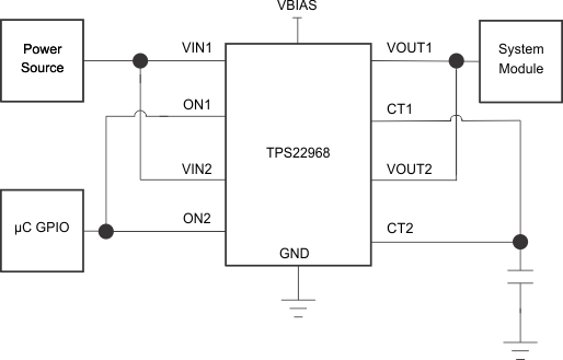 Figure 31. Parallel Configuration
10.1.2 Standby Power Reduction
Any end equipment that is powered from the battery has a need to reduce current consumption to keep the battery charged for a longer time. TPS22968 helps to accomplish this by turning off the supply to the modules that are in standby state, and therefore, significantly reduces the leakage current overhead of the standby modules. See Figure 32.
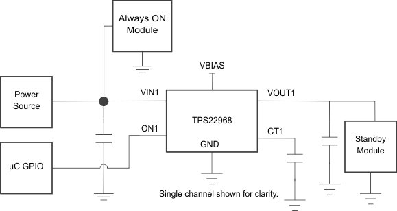 Figure 32. Standby Power Reduction
10.1.3 Power Supply Sequencing Without a GPIO Input
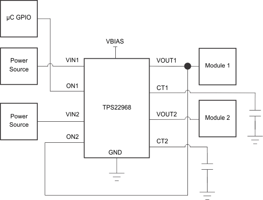
In many end equipments, there is a need to power up various modules in a predetermined manner. The TPS22968 can solve the problem of power sequencing without adding any complexity to the overall system. See Figure 33.
10.1.4 Reverse Current Blocking
In certain applications, it may be desirable to have reverse current blocking. Reverse current blocking prevents current from flowing from the output to the input of the load switch when the device is disabled. With the following configuration, the TPS22968 can be converted into a single-channel switch with reverse current blocking. In this configuration, VIN1 or VIN2 can be used as the input and VIN2 or VIN1 is the output. See Figure 34.
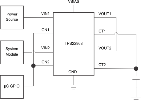 Figure 34. Reverse Current Blocking
10.2 Typical Application
This application demonstrates how the TPS22968 can be used to power downstream modules with large capacitances. The example in Figure 35 TPS22968 is powering a 100-µF capacitive output load.
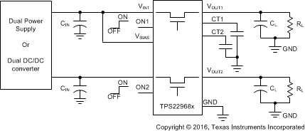 Figure 35. Typical Application Schematic for Powering a Downstream Module
10.2.1 Design Requirements
For this design example, use the following Table 3 as the input parameters.
Table 3. Design Parameters
| DESIGN PARAMETER | EXAMPLE VALUE |
|---|---|
| VIN | 3.3 V |
| VBIAS | 5 V |
| Load current | 4 A |
| Output capacitance (CL) | 22 µF |
| Allowable inrush current on VOUT | 0.33 A |
10.2.2 Detailed Design Procedure
To begin the design process, the designer must know the following:
- VIN voltage
- VBIAS voltage
- Load current
- Allowable inrush current on VOUT due to CL capacitor
10.2.2.1 VIN to VOUT Voltage Drop
The VIN to VOUT voltage drop in the device is determined by the RON of the device and the load current. The RON of the device depends upon the VIN and VBIAS conditions of the device. Refer to the RON specification of the device in the Electrical Characteristics (VBIAS = 5 V) and Electrical Characteristics (VBIAS = 2.5 V) . After the RON of the device is determined based upon the VIN and VBIAS conditions, use Equation 2 to calculate the VIN to VOUT voltage drop:

where
- ΔV is the voltage drop from VIN to VOUT
- ILOAD is the load current
- RON is the On-resistance of the device for a specific VIN and VBIAS combination
An appropriate ILOAD must be chosen such that the IMAX specification of the device is not violated.
10.2.2.2 Inrush Current
To determine how much inrush current is caused by the CL capacitor, use Equation 3.

where
- IINRUSH is the amount of inrush caused by CL
- CL is the capacitance on VOUT
- dt is the time it takes for change in VOUT during the ramp up of VOUT when the device is enabled
- dVOUT is the change in VOUT during the ramp up of VOUT when the device is enabled
The device offers adjustable rise time for VOUT. This feature allows the user to control the inrush current during turnon through the CTx pins. The appropriate rise time can be calculated using the design requirements and the inrush current equation ( Equation 3). See Equation 4 and Equation 5.
To ensure an inrush current of less than 330 mA, choose a CT based on Table 1 or Equation 1 value that yields a rise time of more than 220 µs. See the oscilloscope captures in the Application Curves for an example of how the CT capacitor can be used to reduce inrush current. See Table 1 for correlation between rise times and CT values.
An appropriate CL value must be placed on VOUT such that the IMAX and IPLS specifications of the device are not violated.
10.2.2.3 Thermal Considerations
The maximum IC junction temperature must be restricted to 125°C under normal operating conditions. To calculate the maximum allowable dissipation, PD(max) for a given output current and ambient temperature, use Equation 6.

where
- PD(max) is the maximum allowable power dissipation
- TJ(max) is the maximum allowable junction temperature (125°C for the TPS22968)
- TA is the ambient temperature of the device
- RθJA is the junction to air thermal impedance. See the Thermal Information table. This parameter is highly dependent upon board layout.
Equation 7 to Equation 10 and Equation 11 to Equation 13 show two examples to determine how to use this information correctly:
For VBIAS = 5 V, VIN = 5 V, the maximum ambient temperature with a 4-A load through each channel can be determined by using Equation 7 to Equation 10:
White Space
White Space

White Space
White Space
White Space
For VBIAS = 5 V, VIN = 5 V, the maximum continuous current for an ambient temperature of 85°C with the same current flowing through each channel can be determined by using Equation 11 to Equation 13:
Space

Space

Space

10.2.3 Application Curves
The twp scope captures show the usage of a CT capacitor in conjunction with the device. A higher CT value results in a slower rise and a lower inrush current.
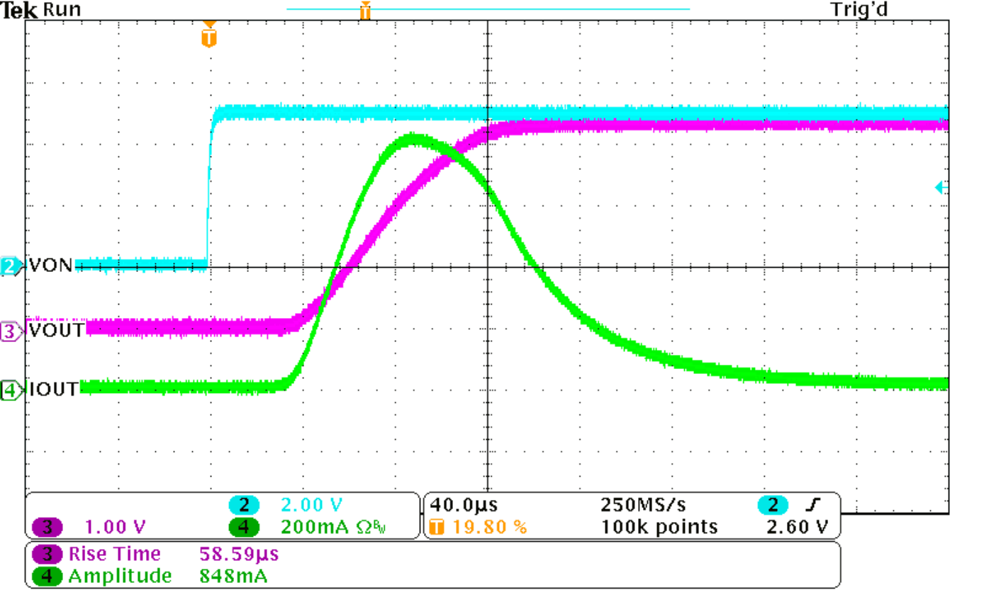
| VBIAS = 5 V | VIN = 3.3 V | TA = 25°C |
| CT = Open |
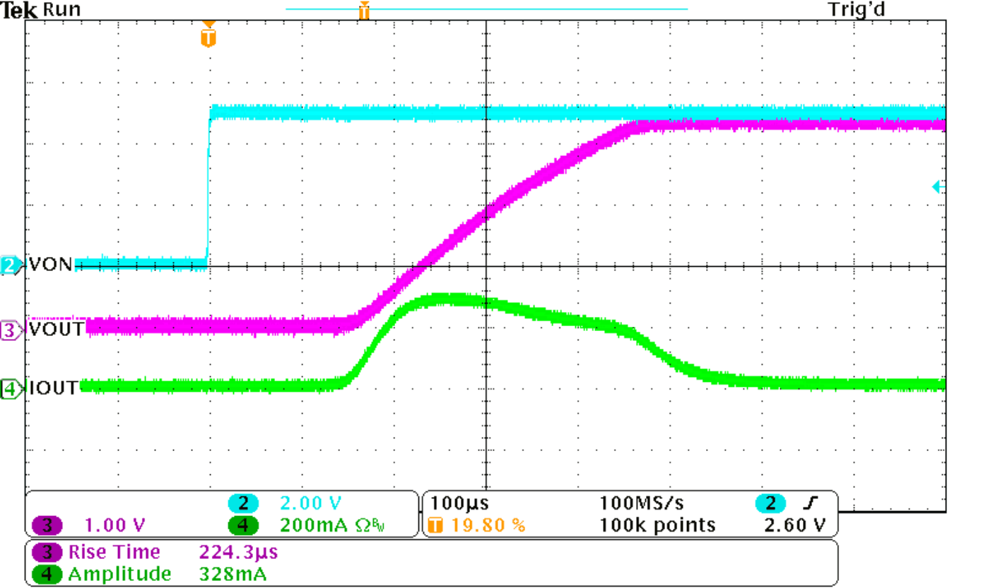
| VBIAS = 5 V | VIN = 3.3 V | TA = 25°C |
| CT = 220 pF |