ZHCSCN4F January   2014  – July 2017 TPS22968

PRODUCTION DATA.  

  1. 特性
  2. 应用
  3. 说明
  4. 修订历史记录
  5. Device Comparison
  6. Pin Configuration and Functions
  7. Specifications
    1. 7.1 Absolute Maximum Ratings
    2. 7.2 ESD Ratings
    3. 7.3 Recommended Operating Conditions
    4. 7.4 Thermal Information
    5. 7.5 Electrical Characteristics (VBIAS = 5 V)
    6. 7.6 Electrical Characteristics (VBIAS = 2.5 V)
    7. 7.7 Switching Characteristics
    8. 7.8 Typical DC Characteristics
    9. 7.9 Typical AC Characteristics
  8. Parameter Measurement Information
  9. Detailed Description
    1. 9.1 Overview
    2. 9.2 Functional Block Diagram
    3. 9.3 Feature Description
      1. 9.3.1 ON and OFF Control
      2. 9.3.2 Input Capacitor (Optional)
      3. 9.3.3 Output Capacitor (Optional)
      4. 9.3.4 QOD (Optional)
      5. 9.3.5 VIN and VBIAS Voltage Range
      6. 9.3.6 Adjustable Rise Time
    4. 9.4 Device Functional Modes
  10. 10Application and Implementation
    1. 10.1 Application Information
      1. 10.1.1 Parallel Configuration
      2. 10.1.2 Standby Power Reduction
      3. 10.1.3 Power Supply Sequencing Without a GPIO Input
      4. 10.1.4 Reverse Current Blocking
    2. 10.2 Typical Application
      1. 10.2.1 Design Requirements
      2. 10.2.2 Detailed Design Procedure
        1. 10.2.2.1 VIN to VOUT Voltage Drop
        2. 10.2.2.2 Inrush Current
        3. 10.2.2.3 Thermal Considerations
      3. 10.2.3 Application Curves
  11. 11Power Supply Recommendations
  12. 12Layout
    1. 12.1 Layout Guidelines
    2. 12.2 Layout Example
  13. 13器件和文档支持
    1. 13.1 器件支持
      1. 13.1.1 开发支持
    2. 13.2 文档支持
      1. 13.2.1 相关文档
    3. 13.3 相关链接
    4. 13.4 接收文档更新通知
    5. 13.5 社区资源
    6. 13.6 商标
    7. 13.7 静电放电警告
    8. 13.8 Glossary
  14. 14机械、封装和可订购信息

封装选项

机械数据 (封装 | 引脚)
散热焊盘机械数据 (封装 | 引脚)
订购信息

Layout

Layout Guidelines

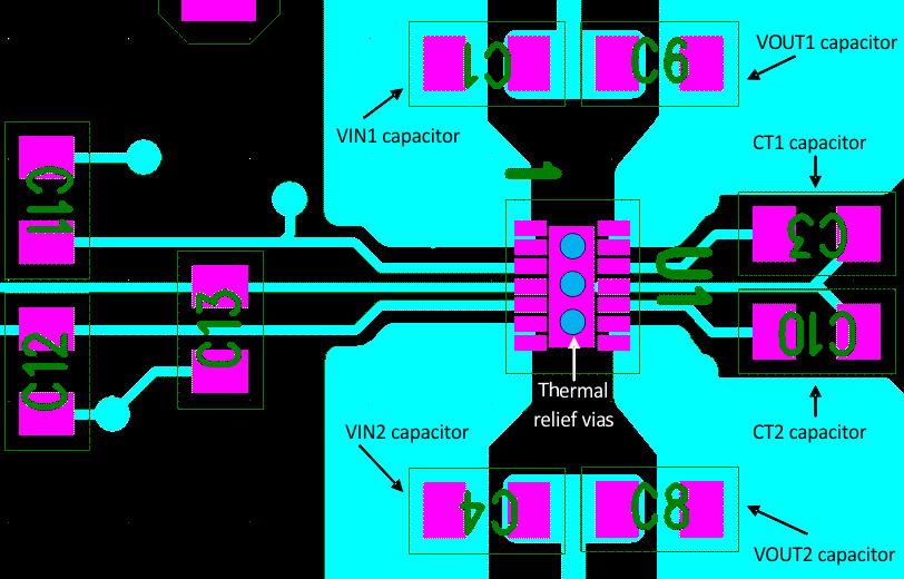
  • VIN and VOUT traces must be as short and wide as possible to accommodate for high current.
  • Use vias under the exposed thermal pad for thermal relief for high current operation.
  • VINx pins must be bypassed to ground with low-ESR ceramic bypass capacitors. The typical recommended bypass capacitance is 1-µF ceramic with X5R or X7R dielectric. This capacitor must be placed as close to the device pins as possible.
  • VOUTx pins must be bypassed to ground with low-ESR ceramic bypass capacitors. The typical recommended bypass capacitance is one-tenth of the VINx bypass capacitor of X5R or X7R dielectric rating. This capacitor must be placed as close to the device pins as possible.
  • The VBIAS pin must be bypassed to ground with low-ESR ceramic bypass capacitors. The typical recommended bypass capacitance is 0.1-µF ceramic with X5R or X7R dielectric.
  • The CTx capacitors must be placed as close to the device pins as possible. The typical recommended CTx capacitance is a capacitor of X5R or X7R dielectric rating with a rating of 25 V or higher.

Layout Example

TPS22968 TPS22968N layout_lvsbh4.gif