ZHCSF87C May 2016 – September 2017 TPS22990
PRODUCTION DATA.
- 1 特性
- 2 应用
- 3 说明
- 4 修订历史记录
- 5 Device Comparison Table
- 6 Pin Configuration and Functions
- 7 Specifications
- 8 Parameter Measurement Information
- 9 Detailed Description
- 10Application and Implementation
- 11Power Supply Recommendations
- 12Layout
- 13器件和文档支持
- 14机械、封装和可订购信息
10 Application and Implementation
NOTE
Information in the following applications sections is not part of the TI component specification, and TI does not warrant its accuracy or completeness. TI’s customers are responsible for determining suitability of components for their purposes. Customers should validate and test their design implementation to confirm system functionality.
10.1 Application Information
10.1.1 Input to Output Voltage Drop
The input to output voltage drop in the device is determined by the RON of the device and the load current. The RON of the device depends upon the VIN and VBIAS condition of the device. See the RON specification in the Electrical Characteristics—VBIAS = 5 V table of this datasheet. Once the RON of the device is determined based upon the VIN and VBIAS conditions, use Equation 3 to calculate the input to output voltage drop.

where
- ΔV is the voltage drop from VIN to VOUT
- ILOAD is the load current
- RON is the on-resistance of the device for a specific VIN and VBIAS
- An appropriate ILOAD must be chosen such that the IMAX specification of the device is not violated
10.1.2 Input Capacitor
It is recommended to use a capacitor between VIN and GND close to the device pins. This helps limit the voltage drop on the input supply caused by transient inrush currents when the switch is turned on into a discharged capacitor at the load. A 1-μF ceramic capacitor, CIN, is usually sufficient. Higher values of CIN can be used to further reduce the voltage drop. A CIN to CL ratio of 10 to 1 is recommended for minimizing VIN dip caused by inrush currents during startup, where CL is the load capacitance.
10.1.3 Thermal Consideration
The maximum junction temperature should be limited to below 125°C. Use Equation 4 to calculate the maximum allowable dissipation, PD(max) for a given output load current and ambient temperature. RθJA is highly dependent upon board layout.

where
- PD(max) is the maximum allowable power dissipation
- TJ(max) is the maximum allowable junction temperature
- TA is the ambient temperature
- RθJA is the junction-to-air thermal impedance
10.1.4 PG Pull Up Resistor
The PG output is an open drain signal which connects to a voltage source through a pull up resistor RPU. The PG signal can be used to drive the enable pins of downstream devices, EN. PG is active high, and its voltage is given by Equation 5.

where
- VOUT is the voltage where PG is tied to
- IPG,LK is the leakage current into PG pin
- IEN,LK is the leakage current into the EN pin driven by PG
- RPU is the pull up resistance
VPG needs to be higher than VIH, MIN of the EN pin to be treated as logic high. The maximum RPU is determined by Equation 6.

When PG is disabled, with 1 mA current into PG pin (IPG = 1 mA), VPG,OL is less than 0.2 V and treated as logic low as long as VIL,MAX of the EN pin is greater than 0.2 V. The minimum RPU is determined by Equation 7.

RPU can be chosen within the range defined by RPU,MIN and RPU,MAX. RPU = 10 kΩ is used for characterization.
10.1.5 Power Sequencing
The TPS22990 has an integrated power good indicator which can be used for power sequencing. As shown in Figure 36, the switch to the second load is controlled by the PG signal from the first switch. This ensures that the power to load 2 is only enabled after the power to load 1 is enabled and the first switch is full load ready.
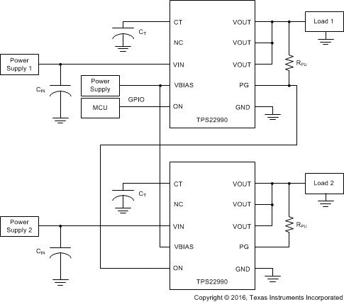 Figure 36. Power Sequencing
10.1.6 Standby Power Reduction
Any end equipment that is being powered from a battery has a need to reduce current consumption in order to maintain the battery charge for a longer time. The TPS22990 devices help to accomplish this reduction by turning off the supply to the downstream modules that are in standby state and significantly reduce the leakage current overhead of the standby modules as shown in Figure 37.
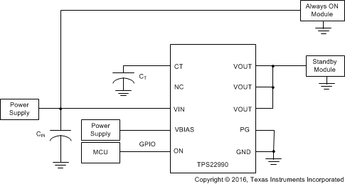 Figure 37. Standby Power Reduction
10.2 Typical Application
Figure 38 demonstrates how to use TPS22990 to limit inrush current to output capacitance.
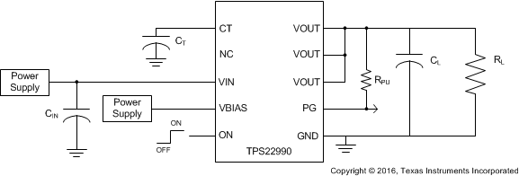 Figure 38. Powering a Downstream Module
10.2.1 Design Requirements
For this design example, use the input parameters shown in Table 4.
Table 4. Design Parameters
| DESIGN PARAMETER | EXAMPLE VALUE |
|---|---|
| VBIAS | 3.3 V |
| VIN | 1.05 V |
| CL | 10 μF |
| RL | None |
| Maximum acceptable inrush current | 100 mA |
10.2.2 Detailed Design Procedure
10.2.2.1 Managing Inrush Current
When the switch is enabled, the output capacitors must be charged up from 0 V to VIN. This charge arrives in the form of inrush current. Inrush current can be calculated using Equation 8.

where
- IINRUSH is the Inrush current
- CL is the Load capacitance
- dV/dt is the Output slew rate
- VIN is the Input voltage
- tR is the rise time
Minimum acceptable rise time can be calculated using the design requirements and the inrush current equation. See Equation 9.

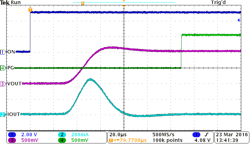
The TPS22990 has very fast timing without a CT capacitor (CT). The typical rise time is 12 μs at VBIAS = 3.3 V, VIN = 1.05 V, RL = 10 Ω, and CL = 0.1 µF. As shown in Figure 39, the rise time is much smaller than 84 µs and the inrush current is 460 mA without CT. The CT for the required rise time must be calculated using Equation 1. For 84 µs, the calculated CT = 5259 pF. Figure 40 shows the inrush current is less than 100 mA with CT = 6800 pF.
10.2.3 Application Curves
