ZHCSGZ0B October 2017 – November 2017 TPS23525
PRODUCTION DATA.
- 1 特性
- 2 应用
- 3 说明
- 4 修订历史记录
- 5 Pin Configuration and Functions
- 6 Specifications
- 7 Parameter Measurement Information
- 8 Detailed Description
-
9 Application and Implementation
- 9.1 Application Information
- 9.2
Typical Application
- 9.2.1 Design Requirements
- 9.2.2
Detailed Design Procedure
- 9.2.2.1 Selecting RSNS
- 9.2.2.2 Selecting Soft Start Setting: CSS and CSS,VEE
- 9.2.2.3 Selecting VDS Switch Over Threshold
- 9.2.2.4 Timer Selection
- 9.2.2.5 MOSFET Selection and SOA Checks
- 9.2.2.6 Input Cap, Input TVS, and OR-ing FET selection
- 9.2.2.7 EMI Filter Consideration
- 9.2.2.8 Under Voltage and Over Voltage Settings
- 9.2.2.9 Choosing RVCC and CVCC
- 9.2.2.10 Power Good Interface to Downstream DC/DC
- 9.2.3 Application Curves
- 10Power Supply Recommendations
- 11Layout
- 12器件和文档支持
- 13机械、封装和可订购信息
8.3.4 OR-ing
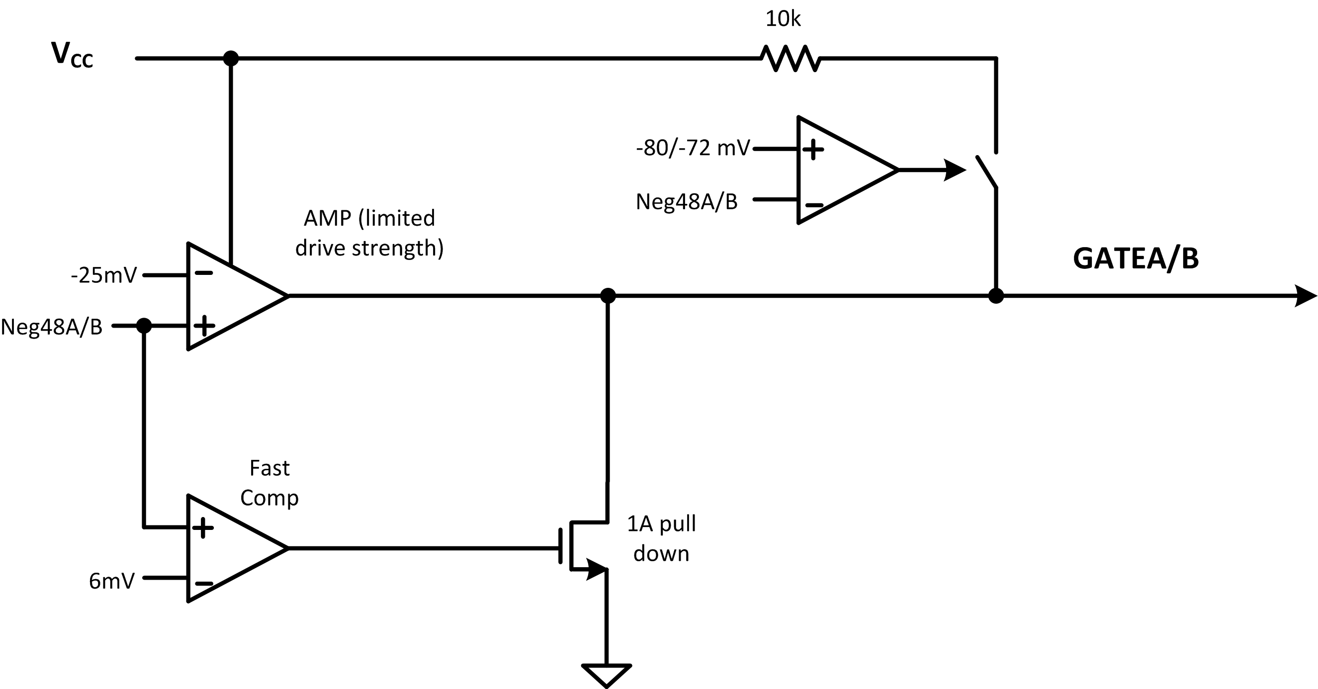
The TPS23525 features integrated OR-ing that controls the external MOSFET in a way to emulate an ideal diode. The TPS23525 will regulate the forward drop across the OR-ing FET to 25 mV. This is accomplished by controlling the VGS of the MOSFET. As the current decreases the VGS is also decreased, which effectively increases the RDSON of the MOSFET. This process is regulated with a low gain amplifier that is gate (OR-ing FET) pole compensated. The lower gain helps ensure stability over various operating conditions. The regulating amplifier ensures that there is no DC reverse current.
However, the amplifier is not very fast and thus it is paired with a fast comparator. This comparator quickly turns off the FET if there is significant reverse current detected.
 Figure 10. Simplified Diagram of OR-ing Block