ZHCSA47E July 2012 – January 2018 TPS23751 , TPS23752
PRODUCTION DATA.
- 1 特性
- 2 应用
- 3 说明
- 4 修订历史记录
- 5 Pin Configuration and Functions
-
6 Specifications
- 6.1 Absolute Maximum Ratings
- 6.2 ESD Ratings
- 6.3 ESD Ratings: Surge
- 6.4 Recommended Operating Conditions
- 6.5 Thermal Information
- 6.6 Electric Characteristics - Controller Section
- 6.7 Electrical Characteristics - Sleep Mode (TPS23752 Only)
- 6.8 Electrical Characteristics - PoE Interface Section
- 6.9 Typical Characteristics
-
7 Detailed Description
- 7.1 Overview
- 7.2 Functional Block Diagrams
- 7.3 Feature Description
- 7.4
Device Functional Modes
- 7.4.1 PoE Overview
- 7.4.2
Sleep Mode Operation (TPS23752 only)
- 7.4.2.1 Converter Controller Features
- 7.4.2.2 PWM and VFO Operation; CTL, SRT, and SRD Pin Relationships to Output Load Current
- 7.4.2.3 Bootstrap Topology
- 7.4.2.4 Current Slope Compensation and Current Limit
- 7.4.2.5 RT
- 7.4.2.6 T2P, Startup and Power Management
- 7.4.2.7 Thermal Shutdown
- 7.4.2.8 Adapter ORing
- 7.4.2.9 Using DEN to Disable PoE
- 7.4.2.10 ORing Challenges
-
8 Application and Implementation
- 8.1 Application Information
- 8.2
Typical Application
- 8.2.1 Design Requirements
- 8.2.2
Detailed Design Procedure
- 8.2.2.1 Input Bridges and Schottky Diodes
- 8.2.2.2 Protection, D1
- 8.2.2.3 Capacitor, C1
- 8.2.2.4 Detection Resistor, RDEN
- 8.2.2.5 Classification Resistor, RCLS
- 8.2.2.6 APD Pin Divider Network, RAPD1, RAPD2
- 8.2.2.7 Setting the PWM-VFO Threshold using the SRT pin
- 8.2.2.8 Setting Frequency (RT)
- 8.2.2.9 Current Slope Compensation
- 8.2.2.10 Voltage Feed-Forward Compensation
- 8.2.2.11 Estimating Bias Supply Requirements and Cvc
- 8.2.2.12 Switching Transformer Considerations and RVC
- 8.2.2.13 T2P Pin Interface
- 8.2.2.14 Softstart
- 8.2.2.15 Special Switching MOSFET Considerations
- 8.2.2.16 ESD
- 8.2.2.17 Thermal Considerations and OTSD
- 8.2.3 Application Curves
- 9 Power Supply Recommendations
- 10Layout
- 11器件和文档支持
- 12机械、封装和可订购信息
7.4.1.2 PoE Startup Sequence
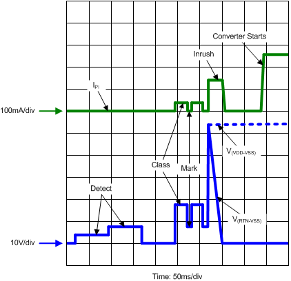
The waveforms of Figure 24 demonstrate detection, classification, and startup from a PSE with type 2 hardware classification. The key waveforms shown are V(VDD-VSS), V(RTN-VSS), and IPI. IEEE 802.3at requires a minimum of two detection levels, two class and mark cycles, and startup from the second mark event. VRTN to VSS falls as the TPS23751 or TPS23752 charges CIN following application of full voltage. Subsequently, the converter starts up, drawing current as seen in the IPI waveform.
 Figure 24. Startup