ZHCSHL4I October 2008 – December 2017 TPS23754 , TPS23754-1 , TPS23756
PRODUCTION DATA.
- 1 特性
- 2 应用
- 3 说明
- 4 修订历史记录
- 5 Pin Configuration and Functions
- 6 Specifications
-
7 Detailed Description
- 7.1 Overview
- 7.2 Functional Block Diagram
- 7.3 Feature Description
- 7.4
Device Functional Modes
- 7.4.1
PoE Overview
- 7.4.1.1 Threshold Voltages
- 7.4.1.2 PoE Start-Up Sequence
- 7.4.1.3 Detection
- 7.4.1.4 Hardware Classification
- 7.4.1.5 Inrush and Start-Up
- 7.4.1.6 Maintain Power Signature
- 7.4.1.7 Start-Up and Converter Operation
- 7.4.1.8 PD Hotswap Operation
- 7.4.1.9 Converter Controller Features
- 7.4.1.10 Bootstrap Topology
- 7.4.1.11 Current Slope Compensation and Current Limit
- 7.4.1.12 Blanking – RBLNK
- 7.4.1.13 Dead Time
- 7.4.1.14 FRS and Synchronization
- 7.4.1.15 T2P, Start-Up, and Power Management
- 7.4.1.16 Thermal Shutdown
- 7.4.1.17 Adapter ORing
- 7.4.1.18 PPD ORing Features
- 7.4.1.19 Using DEN to Disable PoE
- 7.4.1.20 ORing Challenges
- 7.4.1
PoE Overview
-
8 Application and Implementation
- 8.1 Application Information
- 8.2
Typical Application
- 8.2.1 Design Requirements
- 8.2.2
Detailed Design Procedure
- 8.2.2.1 Input Bridges and Schottky Diodes
- 8.2.2.2 Protection, D1
- 8.2.2.3 Capacitor, C1
- 8.2.2.4 Detection Resistor, RDEN
- 8.2.2.5 Classification Resistor, RCLS
- 8.2.2.6 Dead Time Resistor, RDT
- 8.2.2.7 Switching Transformer Considerations and RVC
- 8.2.2.8 Special Switching MOSFET Considerations
- 8.2.2.9 Thermal Considerations and OTSD
- 8.2.2.10 APD Pin Divider Network, RAPD1, RAPD2
- 8.2.2.11 PPD Pin Divider Network, RPPD1, RPPD2
- 8.2.2.12 Setting Frequency (RFRS) and Synchronization
- 8.2.2.13 Current Slope Compensation
- 8.2.2.14 Blanking Period, RBLNK
- 8.2.2.15 Estimating Bias Supply Requirements and CVC
- 8.2.2.16 T2P Pin Interface
- 8.2.2.17 Advanced ORing Techniques
- 8.2.2.18 Soft Start
- 8.2.2.19 Frequency Dithering for Conducted Emissions Control
- 8.2.3 Application Curves
- 9 Power Supply Recommendations
- 10Layout
- 11器件和文档支持
- 12机械、封装和可订购信息
封装选项
请参考 PDF 数据表获取器件具体的封装图。
机械数据 (封装 | 引脚)
- PWP|20
散热焊盘机械数据 (封装 | 引脚)
- PWP|20
订购信息
6.8 Typical Characteristics
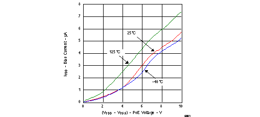 Figure 2. Detection Bias Current vs Voltage
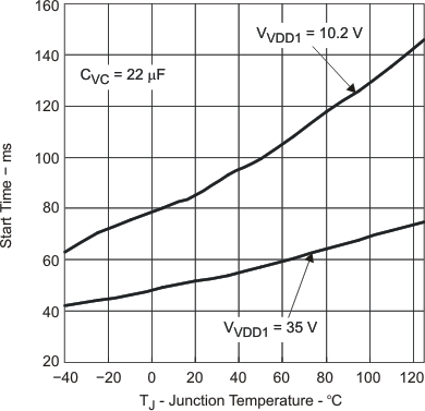
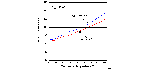 Figure 4. '754 Converter Start Time vs Temperature
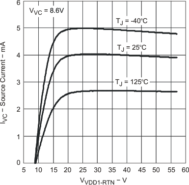
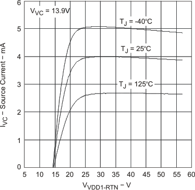 Figure 6. '754 Converter Start-Up Current vs VVDD1
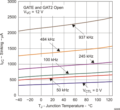 Figure 8. Controller Bias Current vs Temperature
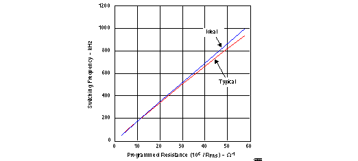 Figure 12. Switching Frequency vs Program Conductance
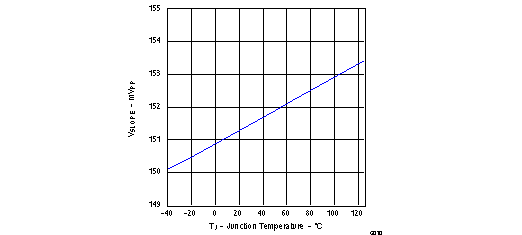 Figure 14. Current Slope Compensation Voltage vs Temperature
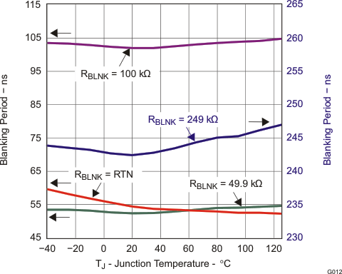 Figure 16. Blanking Period vs Temperature
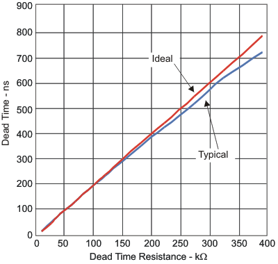 Figure 18. Dead Time vs Dead Time Resistance (RDT )
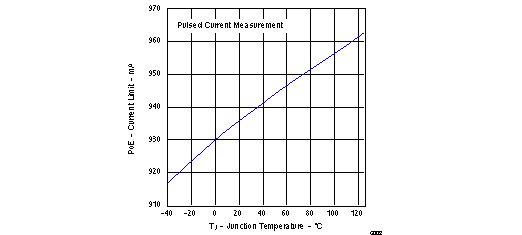 Figure 3. PoE Current Limit vs Temperature
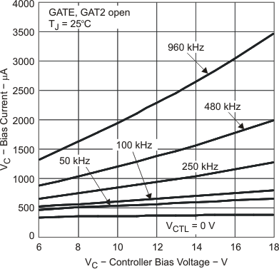
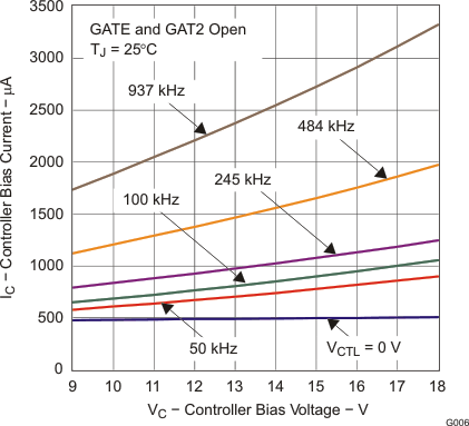 Figure 9. '754 Controller Bias Current vs Voltage
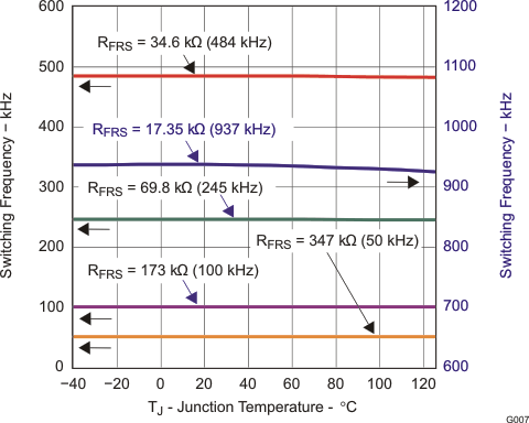 Figure 11. Switching Frequency vs Temperature
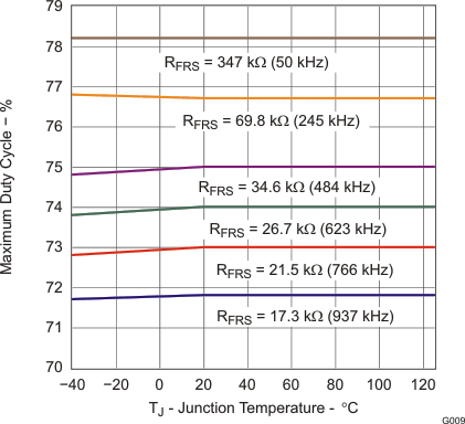 Figure 13. Maximum Duty Cycle vs Temperature
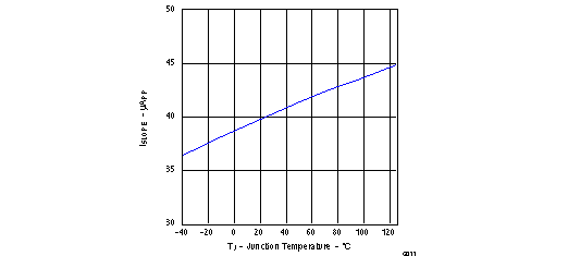 Figure 15. Current Slope Compensation Current vs Temperature
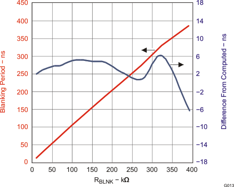 Figure 17. Blanking Period vs Blanking Resistance (RBLNK)
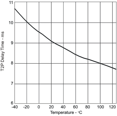 Figure 19. T2P Delay Time vs Temperature
