ZHCS845A March 2012 – July 2015 TPS2379
PRODUCTION DATA.
- 1 特性
- 2 应用
- 3 说明
- 4 修订历史记录
- 5 Pin Configuration and Functions
- 6 Specifications
- 7 Parameter Measurement Information
-
8 Detailed Description
- 8.1 Overview
- 8.2 Functional Block Diagram
- 8.3 Feature Description
- 8.4
Device Functional Modes
- 8.4.1
PoE Overview
- 8.4.1.1 Threshold Voltages
- 8.4.1.2 PoE Start-Up Sequence
- 8.4.1.3 Detection
- 8.4.1.4 Hardware Classification
- 8.4.1.5 Inrush and Start-up
- 8.4.1.6 Maintain Power Signature
- 8.4.1.7 Start-up and Operation
- 8.4.1.8 PD Hotswap Operation
- 8.4.1.9 CDB and T2P
- 8.4.1.10 Auxiliary Pass MOSFET Control
- 8.4.1.11 Using DEN to Disable PoE
- 8.4.1
PoE Overview
- 9 Application and Implementation
- 10Power Supply Recommendations
- 11Layout
- 12器件和文档支持
- 13机械、封装和可订购信息
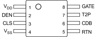
5 Pin Configuration and Functions
DDA Package
8-Pin HSOP
Top View

Pin Functions
| PIN | I/O | DESCRIPTION | |
|---|---|---|---|
| NAME | NO. | ||
| VDD | 1 | I | Connect to positive PoE input power rail. Bypass with 0.1 µF to VSS. |
| DEN | 2 | I/O | Connect 24.9 kΩ to VDD for detection. Pull to VSS disable pass MOSFET. |
| CLS | 3 | O | Connect resistor from CLS to VSS to program classification current. |
| VSS | 4 | — | Connect to negative power rail derived from PoE source. |
| RTN | 5 | O | Drain of PoE pass MOSFET. |
| CDB | 6 | O | Opendrain converter disable output, active low, referenced to RTN. |
| T2P | 7 | O | Active low indicates type 2 PSE connected. |
| GATE | 8 | O | Auxiliary gate driver output. |
| PowerPAD | — | — | The PowerPAD must be connected to VSS. A large fill area is required to assist in heat dissipation. |