ZHCSCE7I March 2014 – July 2019 TPS23861
PRODUCTION DATA.
- 1 特性
- 2 应用范围
- 3 说明
- 4 修订历史记录
- 5 Pin Configuration and Functions
- 6 Specifications
-
7 Detailed Description
- 7.1 Overview
- 7.2 Functional Block Diagram
- 7.3
Feature Description
- 7.3.1 Detection Resistance Measurement
- 7.3.2 Physical Layer Classification
- 7.3.3 Class and Detect Fields
- 7.3.4 Register State Following a Fault
- 7.3.5 Disconnect
- 7.3.6 Disconnect Threshold
- 7.3.7 Fast Shutdown Mode
- 7.3.8 Legacy Device Detection
- 7.3.9 VPWR Undervoltage and UVLO Events
- 7.3.10 Timer-Deferrable Interrupt Support
- 7.3.11 A/D Converter and I2C Interface
- 7.3.12 Independent Operation when the AUTO Bit is Set
- 7.3.13 I2C Slave Address and AUTO Bit Programming
- 7.4 Device Functional Modes
- 7.5
Register Map – I2C-Addressable
- 7.5.1 Interrupt Register
- 7.5.2 Interrupt Enable Register
- 7.5.3 Power Event Register
- 7.5.4 Detection Event Register
- 7.5.5 Fault Event Register
- 7.5.6 Start/ILIM Event Register
- 7.5.7 Supply Event Register
- 7.5.8 Port n Status Register
- 7.5.9 Power Status Register
- 7.5.10 I2C Slave Address Register
- 7.5.11 Operating Mode Register
- 7.5.12 Disconnect Enable Register
- 7.5.13 Detect/Class Enable Register
- 7.5.14 Port Power Priority Register
- 7.5.15 Timing Configuration Register
- 7.5.16 General Mask 1 Register
- 7.5.17 Detect/Class Restart Register
- 7.5.18 Power Enable Register
- 7.5.19 Reset Register
- 7.5.20 Legacy Detect Mode Register
- 7.5.21 Two-Event Classification Register
- 7.5.22 Interrupt Timer Register
- 7.5.23 Disconnect Threshold Register
- 7.5.24 ICUTnm CONFIG Register
- 7.5.25 Temperature Register
- 7.5.26 Input Voltage Register
- 7.5.27 Port n Current Register
- 7.5.28 Port n Voltage Register
- 7.5.29 PoE Plus Register
- 7.5.30 Firmware Revision Register
- 7.5.31 I2C Watchdog Register
- 7.5.32 Device ID Register
- 7.5.33 Cool Down/Gate Drive Register
- 7.5.34 Port n Detect Resistance Register
- 7.5.35 Port n Detect Voltage Difference Register
- 7.5.36 Reserved Registers
-
8 Application and Implementation
- 8.1 Introduction to PoE
- 8.2 Application Information
- 8.3 Typical Application
- 8.4 System Examples
- 9 Power Supply Recommendations
- 10Layout
- 11器件和文档支持
- 12机械、封装和可订购信息
8.4.4 Foldback Protection (ILIM)
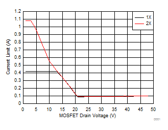
The TPS23861 features two types of foldback protection mechanisms for complete MOSFET protection. During inrush at port power on, the foldback is based on the port voltage as shown in Figure .
NOTE
The inrush-current profile remains the same no matter what the state is of the PoEPn bit in the PoE Plus Register.
After the port has been powered on and Power Good is valid, a dual-slope foldback current limit is applied, providing protection against partial and total short-circuit at port output, while still being able to maintain the port powered during normal transients in the TPS23861 input voltage or load current. Refer to Figure 58. Note that setting the POEPn bit selects the 2x curve while clearing it selects the 1x curve.
The TLIM timer starts counting down when the current-limit threshold in Figure 57 and Figure 58 is reached. When it reaches zero the port is powered down. If the ILIM current-limit condition is cleared while the TLIM timer is counting, the TLIM timer counts up, at a slower rate, without exceeding the maximum count corresponding to the setting in the TLIM field which is located in the Timing Configuration Register.
If the port experiences a short circuit, the TPS23861 forces zero volts on the gate of the external FET to protect it from destruction. Within microseconds the foldback circuit engages, and until the ILIM timeout is reached, the port current is controlled according to the foldback schedule.
The ILIM current limit is to be applied such that its setting is greater than the setting of the ICUT current threshold. That is, an ICUT current-limit condition should occur before the TPS23861 asserts foldback control over the port current via an ILIM current limit. To this end, the ILIM current limit must be set greater than the ICUT current threshold. This must be accomplished by the host except when in Auto Mode (or the AUTO bit is set). In that case, the settings for ICUT and ILIM will be properly set based on classification results before the port is powered on.
