ZHCSCE7I March 2014 – July 2019 TPS23861
PRODUCTION DATA.
- 1 特性
- 2 应用范围
- 3 说明
- 4 修订历史记录
- 5 Pin Configuration and Functions
- 6 Specifications
-
7 Detailed Description
- 7.1 Overview
- 7.2 Functional Block Diagram
- 7.3
Feature Description
- 7.3.1 Detection Resistance Measurement
- 7.3.2 Physical Layer Classification
- 7.3.3 Class and Detect Fields
- 7.3.4 Register State Following a Fault
- 7.3.5 Disconnect
- 7.3.6 Disconnect Threshold
- 7.3.7 Fast Shutdown Mode
- 7.3.8 Legacy Device Detection
- 7.3.9 VPWR Undervoltage and UVLO Events
- 7.3.10 Timer-Deferrable Interrupt Support
- 7.3.11 A/D Converter and I2C Interface
- 7.3.12 Independent Operation when the AUTO Bit is Set
- 7.3.13 I2C Slave Address and AUTO Bit Programming
- 7.4 Device Functional Modes
- 7.5
Register Map – I2C-Addressable
- 7.5.1 Interrupt Register
- 7.5.2 Interrupt Enable Register
- 7.5.3 Power Event Register
- 7.5.4 Detection Event Register
- 7.5.5 Fault Event Register
- 7.5.6 Start/ILIM Event Register
- 7.5.7 Supply Event Register
- 7.5.8 Port n Status Register
- 7.5.9 Power Status Register
- 7.5.10 I2C Slave Address Register
- 7.5.11 Operating Mode Register
- 7.5.12 Disconnect Enable Register
- 7.5.13 Detect/Class Enable Register
- 7.5.14 Port Power Priority Register
- 7.5.15 Timing Configuration Register
- 7.5.16 General Mask 1 Register
- 7.5.17 Detect/Class Restart Register
- 7.5.18 Power Enable Register
- 7.5.19 Reset Register
- 7.5.20 Legacy Detect Mode Register
- 7.5.21 Two-Event Classification Register
- 7.5.22 Interrupt Timer Register
- 7.5.23 Disconnect Threshold Register
- 7.5.24 ICUTnm CONFIG Register
- 7.5.25 Temperature Register
- 7.5.26 Input Voltage Register
- 7.5.27 Port n Current Register
- 7.5.28 Port n Voltage Register
- 7.5.29 PoE Plus Register
- 7.5.30 Firmware Revision Register
- 7.5.31 I2C Watchdog Register
- 7.5.32 Device ID Register
- 7.5.33 Cool Down/Gate Drive Register
- 7.5.34 Port n Detect Resistance Register
- 7.5.35 Port n Detect Voltage Difference Register
- 7.5.36 Reserved Registers
-
8 Application and Implementation
- 8.1 Introduction to PoE
- 8.2 Application Information
- 8.3 Typical Application
- 8.4 System Examples
- 9 Power Supply Recommendations
- 10Layout
- 11器件和文档支持
- 12机械、封装和可订购信息
6.7 Switching Characteristics
–40 ≤ TJ ≤ +125°C, VVDD = 3.3 V, VVPWR = 48 V, VDGND = VAGND, DGND, KSENSA and KSENSB connected to AGND, and all outputs are unloaded, PoEPn = 0, Positive currents are into pins, RS = 0.255 Ω, to KSENSA (SEN1 or SEN2) or to KSENSB (SEN3 or SEN4), RSENS = 22 Ω, RDRAIN = 47 Ω, typical values are at 25°C. All voltages are with respect to AGND, operating registers loaded with default values (unless otherwise noted)| PARAMETER | TEST CONDITIONS | MIN | TYP | MAX | UNIT | |
|---|---|---|---|---|---|---|
| δIfault | Duty cycle of IPORT with current fault | 5.5% | 6.7% | |||
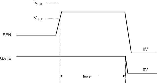
| tOVLD | ICUT time limit | TICUT = 00, default as supplied | 50 | 70 | ms | |
| TICUT = 01 | 25 | 35 | ms | |||
| TICUT = 10 | 100 | 140 | ms | |||
| TICUT = 11 | 200 | 280 | ms | |||
| tLIM | ILIM time limit | POEPn = 0, default as supplied | 50 | 70 | ms | |
| POEPn = 1, TLIM = 00 | 50 | 70 | ms | |||
| POEPn = 1, TLIM = 01 | 28.4 | 30 | 34 | ms | ||
| POEPn = 1, TLIM = 10 | 14.7 | 15.5 | 17 | ms | ||
| POEPn = 1, TLIM = 11 | 9.025 | 11.5 | ms | |||
| tSTART | Maximum current limit duration in port start-up | TSTART = 00, default as supplied | 50 | 70 | ms | |
| TSTART = 01 | 25 | 35 | ms | |||
| TSTART = 10 | 100 | 140 | ms | |||
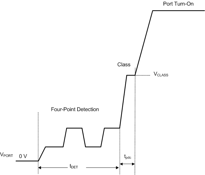
| tDET | Four-point detection duration | Time to complete a detection | 275 | 500 | ms | |
| tDET_BOFF | Pause between detection attempts | VVPWR – VDRAINn > 2.5 V | 300 | 400 | 500 | ms |
| VVPWR – VDRAINn < 2.5 V | 0 | 150 | ms | |||
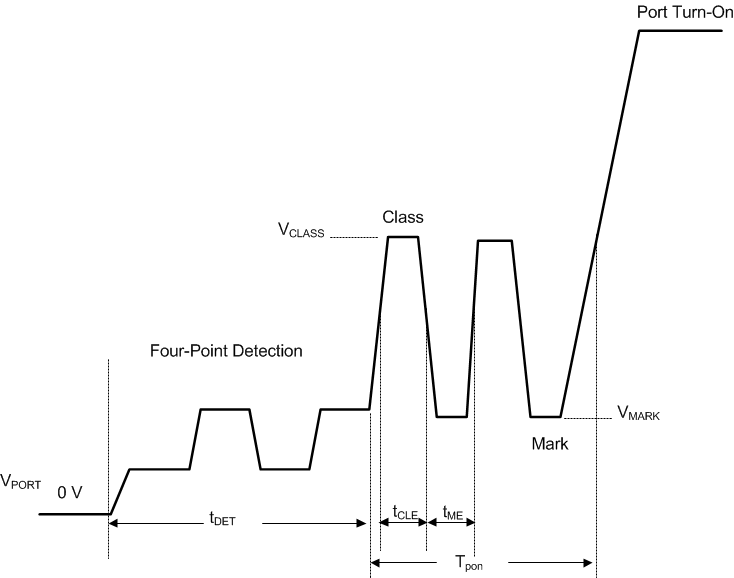
| tCLE | Classification duration | 1st and 2nd class event, Auto Mode, Semi-Auto Mode, from detection complete | 6.5 | 13 | ms | |
| tpdc | Classification duration | 1-event physical layer class timing, Auto Mode and Semi-Auto Mode, from detection complete | 6.5 | 13 | ms | |
| Manual mode, from beginning of classification | 6.5 | 14 | ms | |||
| tME | Mark duration | 1st and 2nd mark event, from class 4 complete | 6 | 12 | ms | |
| tp(on) | Port power-on delay | Manual mode, from port turn-on command to port turn on completed | 4 | ms | ||
| ted | Fault delay timing. Delay before next attempt to power a port following power removal due to fault condition | ICUT , ILIM or start fault, Auto Mode, Semi-Auto Mode,
CLDN = 0X, default as supplied |
0.8 | 1 | 1.2 | s |
| ICUT , ILIM or start fault, Auto Mode, Semi-Auto Mode,
CLDN = 10 |
1.6 | 2 | 2.4 | s | ||
| ICUT , ILIM or start fault, Auto Mode, Semi-Auto Mode,
CLDN = 11 |
3.2 | 4 | 4.8 | s | ||
| tMPDO | PD maintain power signature dropout time limit | TDIS = 00, default as supplied | 300 | 400 | ms | |
| TDIS = 01 | 75 | 100 | ms | |||
| TDIS = 10 | 150 | 200 | ms | |||
| TDIS = 11 | 600 | 800 | ms | |||
| tD_off_SHDWN | Gate turn-off time from SHTDWN input | From SHTDWN to VGATEn < 1 V, VSENn = 0 V | 1 | 5 | µs | |
| tP_off_CMD | Gate turn-off time from port off command | From port off command to VGATEn < 1 V, VSENn = 0 V | 900 | µs | ||
| tP_off_RST | Gate turn-off time with RESET pin | From RESET low to, VGATEn < 1 V, VSENn = 0 V | 1 | 5 | µs | |
| tD_off_SEN | Gate turn-off time from SENn input | POEPn = 0,
VDRAINn = 1 V , from VSENn pulsed to 0.425 V |
0.9 | µs | ||
| POEPn = 1,
VDRAINn = 1 V , from VSENn pulsed to 0.62 V |
0.9 | µs | ||||
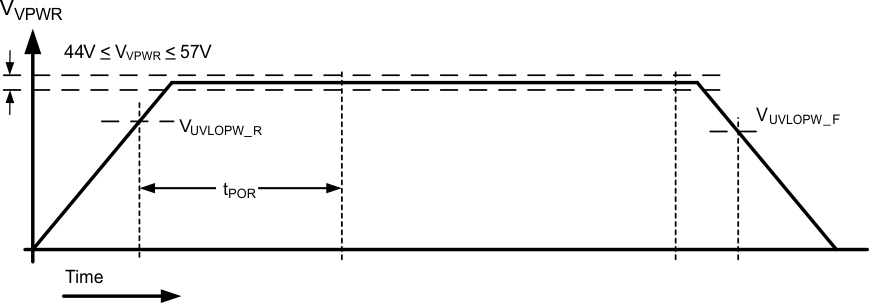
| tPOR | Device power-on-reset delay | 23 | ms | |||
| tRESET | Reset time duration from RESET pin | 1 | 5 | µs | ||
 Figure 2. Overcurrent Fault Timing
  Figure 3. Detection, 1-Event Classification, and Turn On
  Figure 4. Detection, 2-Event Classification, and Turn On
For more information refer to the application note, TPS23861 Power-On Considerations, SLVA723.
Figure 5. VDD Power-On-Reset 
For more information refer to the application note, TPS23861 Power-On Considerations, SLVA723.
Figure 6. VPWR Power-On-Reset