SLUS599B June   2004  – October  2015 TPS2400

PRODUCTION DATA.  

  1. Features
  2. Applications
  3. Description
  4. Revision History
  5. Pin Configuration and Functions
  6. Specifications
    1. 6.1 Absolute Maximum Ratings
    2. 6.2 ESD Ratings
    3. 6.3 Recommended Operating Conditions
    4. 6.4 Thermal Information
    5. 6.5 Electrical Characteristics
    6. 6.6 Typical Characteristics
  7. Parameter Measurement Information
  8. Detailed Description
    1. 8.1 Overview
    2. 8.2 Functional Block Diagram
    3. 8.3 Feature Description
      1. 8.3.1 Undervoltage and Overvoltage Comparators and Logic
      2. 8.3.2 Charge Pump
      3. 8.3.3 Zener Diodes
      4. 8.3.4 Shut-Off MOSFET
    4. 8.4 Device Functional Modes
      1. 8.4.1 Overvoltage Protection
  9. Application and Implementation
    1. 9.1 Application Information
    2. 9.2 Typical Applications
      1. 9.2.1 TPS2400 Application
        1. 9.2.1.1 Design Requirements
        2. 9.2.1.2 Detailed Design Procedure
          1. 9.2.1.2.1 Controlling the Load Inrush-Current
        3. 9.2.1.3 Application Curve
      2. 9.2.2 High-Side Switch Overvoltage Protector That Can Drive a 12−V Load
      3. 9.2.3 Low−Side Switch Overvoltage Protector That Can Drive a 12−V Load
  10. 10Power Supply Recommendations
  11. 11Layout
    1. 11.1 Layout Guidelines
    2. 11.2 Layout Example
  12. 12Device and Documentation Support
    1. 12.1 Documentation Support
      1. 12.1.1 Related Documentation
    2. 12.2 Community Resources
    3. 12.3 Trademarks
    4. 12.4 Electrostatic Discharge Caution
    5. 12.5 Glossary
  13. 13Mechanical, Packaging, and Orderable Information

封装选项

请参考 PDF 数据表获取器件具体的封装图。

机械数据 (封装 | 引脚)
  • DBV|5
散热焊盘机械数据 (封装 | 引脚)
订购信息

5 Pin Configuration and Functions

DBV Package
5-Pin SOT-23
Top View
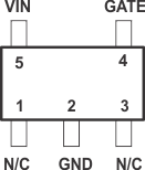
TPS2400 po_slus599.gif

Pin Functions

PIN I/O DESCRIPTION
NAME NO.
GATE 4 O Output gate drive for an external N-channel MOSFET
GND 2 Ground
NC 1, 3 No internal connection
VIN 5 I Input voltage