ZHCSKC1D January 2007 – October 2019 TPS2412 , TPS2413
PRODUCTION DATA.
- 1 特性
- 2 应用
- 3 说明
- 4 修订历史记录
- 5 Device Comparison Table
- 6 Pin Configuration and Functions
- 7 Specifications
-
8 Detailed Description
- 8.1 Overview
- 8.2 Functional Block Diagram
- 8.3
Feature Description
- 8.3.1 Definitions
- 8.3.2 TPS2412 vs TPS2413 – MOSFET Control Methods
- 8.3.3 N+1 Power Supply – Typical Connection
- 8.3.4 Input ORing – Typical Connection
- 8.3.5 System Design and Behavior With Transients
- 8.3.6 TPS2412 Regulation-Loop Stability
- 8.3.7 MOSFET Selection and R(RSET)
- 8.3.8 Gate Drive, Charge Pump and C(BYP)
- 8.4 Device Functional Modes
- 9 Application and Implementation
- 10Power Supply Recommendations
- 11Layout
- 12器件和文档支持
- 13机械、封装和可订购信息
请参考 PDF 数据表获取器件具体的封装图。
机械数据 (封装 | 引脚)
- D|8
- PW|8
散热焊盘机械数据 (封装 | 引脚)
8.1 Overview
The TPS2412/13 is designed to allow an output ORing in N+1 power supply applications (see Figure 9), and an input-power bus ORing in redundant source applications (see Figure 10). The TPS2412/13 and external MOSFET emulate a discrete diode to perform this unidirectional power combining function. The advantage to this emulation is lower forward voltage drop and the ability to tune the operation.
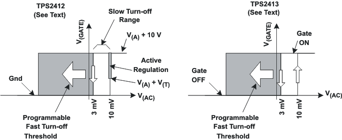
The TPS2412 turns the MOSFET on with a linear control loop that regulates V(AC) to 10 mV as shown in Figure 8. With the gate low, and V(AC) increasing to 10 mV, the amplifier drives GATE high with all available output current until regulation is reached. The regulator controls V(GATE) to maintain V(AC) at 10 mV as long as the MOSFET rDS(on) × I(DRAIN) is less than this the regulated voltage. The regulator drives GATE high, turning the MOSFET fully ON when the rDS(on) × I(DRAIN) exceeds 10 mV; otherwise, V(GATE) will be near V(A) plus the MOSFET gate threshold voltage. If the external circuits force V(AC) below 10 mV and above the programmed fast turnoff, GATE is slowly turned off. GATE is rapidly pulled to ground if V(AC) falls to the RSET programmed fast turnoff threshold.
The TPS2413 turns the MOSFET on and off like a comparator with hysteresis as shown in Figure 8. GATE is driven high when V(AC) exceeds 10 mV, and rapidly turned off if V(AC) falls to the RSET programmed fast turnoff threshold.
System designs should account for the inherent delay between a TPS2412/13 circuit becoming forward biased, and the MOSFET actually turning ON. The delay is the result of the MOSFET gate capacitance charge from ground to its threshold voltage by the 290 μA gate current. If there are no additional sources holding the ORed rail voltage up, the MOSFET internal diode will conduct and maintain voltage on the ORed output, but there will be some voltage droop. This condition is analogous to the power source being ORed in this case. The DC-DC converter output voltage droops when its load increases from zero to a high value. Load sharing techniques that keep all ORed sources active solve this condition.
 Figure 8. TPS241x Operation
 The operation of the two parts is summarized in Table 1.
Table 1. Operation as a Function of VAC
| PART | V(AC) ≤ TURNOFF THRESHOLD(1) | TURNOFF THRESHOLD(1) ≤ VAC ≤ 10 mV | V(AC) > 10 mV | |
|---|---|---|---|---|
| V(AC) FORCED < 10 mV | (MOSFET
rDS(on) × ILOAD) ≤ 10 mV |
|||
| TPS2412 | Strong GATE pulldown (OFF) | Weak GATE pulldown (OFF) | V(AC) regulated to 10 mV | GATE pulled high (ON) |
| TPS2413 | Strong GATE pulldown (OFF) | Depends on previous state (Hysteresis region) | GATE pulled high (ON) | |