ZHCS033G January 2011 – November 2015 TPS24710 , TPS24711 , TPS24712 , TPS24713
PRODUCTION DATA.
- 1 特性
- 2 应用
- 3 说明
- 4 修订历史记录
- 5 Device Comparison Table
- 6 Pin Configuration and Functions
- 7 Specifications
- 8 Detailed Description
-
9 Application and Implementation
- 9.1 Application Information
- 9.2
Typical Application
- 9.2.1 Design Requirements
- 9.2.2
Detailed Design Procedure
- 9.2.2.1
Power-Limited Start-Up
- 9.2.2.1.1 STEP 1. Choose RSENSE
- 9.2.2.1.2 STEP 2. Choose MOSFET M1
- 9.2.2.1.3 STEP 3. Choose Power-Limit Value, PLIM, and RPROG
- 9.2.2.1.4 STEP 4. Choose Output Voltage Rising Time, tON, CT
- 9.2.2.1.5 STEP 5. Calculate the Retry-Mode Duty Ratio
- 9.2.2.1.6 STEP 6. Select R1 and R2 for UV
- 9.2.2.1.7 STEP 7. Choose RGATE, R4, R5 and C1
- 9.2.2.2 Additional Design Considerations
- 9.2.2.1
Power-Limited Start-Up
- 9.2.3 Application Curve
- 10Power Supply Recommendations
- 11Layout
- 12器件和文档支持
- 13机械、封装和可订购信息
7 Specifications
7.1 Absolute Maximum Ratings
over operating free-air temperature range, all voltages referred to GND (unless otherwise noted) (1)| MIN | MAX | UNIT | |||
|---|---|---|---|---|---|
| Input voltage range | EN, FLT(2)(3), FLTb(2)(4), GATE, OUT, PG(2)(3), PGb(2)(4), SENSE, VCC | –0.3 | 30 | V | |
| PROG(2) | –0.3 | 3.6 | |||
| SENSE to VCC | –0.3 | 0.3 | |||
| TIMER | –0.3 | 5 | |||
| Sink current | FLT, PG, FLTb, PGb | 5 | mA | ||
| Source current | PROG | Internally limited | |||
| Temperature | Maximum junction, TJ | Internally limited | °C | ||
(1) Stresses beyond those listed under Absolute Maximum Ratings may cause permanent damage to the device. These are stress ratings only, which do not imply functional operation of the device at these or any other conditions beyond those indicated under Recommended Operating Conditions. Exposure to absolute-maximum-rated conditions for extended periods may affect device reliability.
(2) Do not apply voltages directly to these pins.
(3) for TPS24712/13
(4) for TPS24710/11
7.2 ESD Ratings
| VALUE | UNIT | ||||
|---|---|---|---|---|---|
| V(ESD) | Electrostatic discharge | Human-body model (HBM), per ANSI/ESDA/JEDEC JS-001(1) | All pins except PG and PGb | ±2000 | V |
| PG, PGb | ±500 | V | |||
| Charged-device model (CDM), per JEDEC specification JESD22-C101(2) | ±500 | V | |||
(1) JEDEC document JEP155 states that 500-V HBM allows safe manufacturing with a standard ESD control process.
(2) JEDEC document JEP157 states that 250-V CDM allows safe manufacturing with a standard ESD control process.
7.3 Recommended Operating Conditions
over operating free-air temperature range (unless otherwise noted)| MIN | NOM | MAX | UNIT | ||
|---|---|---|---|---|---|
| Input voltage range | SENSE, VCC | 2.5 | 18 | V | |
| EN, FLT, FLTb, PG, PGb, OUT | 0 | 18 | |||
| Sink current | FLT, FLTb, PG, PGb | 0 | 2 | mA | |
| Resistance | PROG | 4.99 | 500 | kΩ | |
| External capacitance | TIMER | 1 | nF | ||
| Operating junction temperature range, TJ | –40 | 125 | °C | ||
7.4 Thermal Information
| THERMAL METRIC(1) | TPS2471/x | UNIT | |
|---|---|---|---|
| MSOP (10) PINS | |||
| RθJA | Junction-to-ambient thermal resistance | 166.5 | °C/W |
| RθJC(top) | Junction-to-case (top) thermal resistance | 41.8 | |
| RθJB | Junction-to-board thermal resistance | 86.1 | |
| ψJT | Junction-to-top characterization parameter | 1.5 | |
| ψJB | Junction-to-board characterization parameter | 84.7 | |
| RθJC(bot) | Junction-to-case (bottom) thermal resistance | n/a | |
(1) For more information about traditional and new thermal metrics, see the IC Package Thermal Metrics application report, SPRA953.
7.5 Electrical Characteristics
–40°C ≤ TJ ≤ 125°C, VCC = 12 V, VEN = 3 V, and RPROG = 50 kΩ to GND.All voltages referenced to GND, unless otherwise noted.
| PARAMETER | CONDITIONS | MIN | NOM | MAX | UNIT |
|---|---|---|---|---|---|
| VCC | |||||
| UVLO threshold, rising | 2.2 | 2.32 | 2.45 | V | |
| UVLO threshold, falling | 2.1 | 2.22 | 2.35 | V | |
| UVLO hysteresis(1) | 0.1 | V | |||
| Supply current | Enabled ― IOUT + IVCC + ISENSE | 1 | 1.4 | mA | |
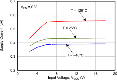
| Disabled(1) ― EN = 0 V, IOUT + IVCC + ISENSE | 0.45 | mA | |||
| EN | |||||
| Threshold voltage, falling | 1.2 | 1.3 | 1.4 | V | |
| Hysteresis(1) | 50 | mV | |||
| Input leakage current | 0 V ≤ VEN ≤ 30 V | –1 | 0 | 1 | µA |
| FLT, FLTb | |||||
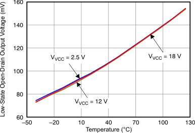
| Output low voltage | Sinking 2 mA | 0.11 | 0.25 | V | |
| Input leakage current | VFLT = 0 V, 30 V | –1 | 0 | 1 | µA |
| VFLTb = 0 V, 30 V | |||||
| PG, PGb | |||||
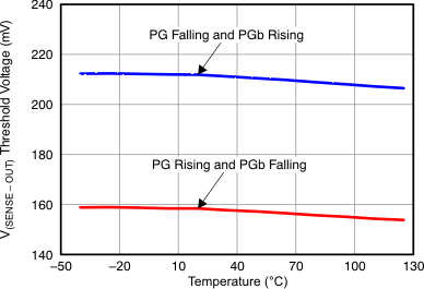
| Threshold | V(SENSE – OUT) rising, PG going low | 140 | 240 | 340 | mV |
| V(SENSE – OUT) rising, PGb going high | |||||
| Hysteresis(1) | Measured V(SENSE – OUT) falling, PG going high | 70 | mV | ||
| Measured V(SENSE – OUT) falling, PGb going low | |||||
| Output low voltage | Sinking 2 mA | 0.11 | 0.25 | V | |
| Input leakage current | VPG = 0 V, 30 V | –1 | 0 | 1 | µA |
| VPGb = 0 V, 30 V | |||||
| PROG | |||||
| Bias voltage | Sourcing 10 µA | 0.65 | 0.678 | 0.7 | V |
| Input leakage current | VPROG = 1.5 V | –0.2 | 0 | 0.2 | µA |
| TIMER | |||||
| Sourcing current | VTIMER = 0 V | 8 | 10 | 12 | µA |
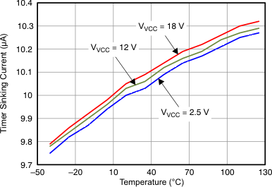
| Sinking current | VTIMER = 2 V | 8 | 10 | 12 | µA |
| VEN = 0 V, VTIMER = 2 V | 2 | 4.5 | 7 | mA | |
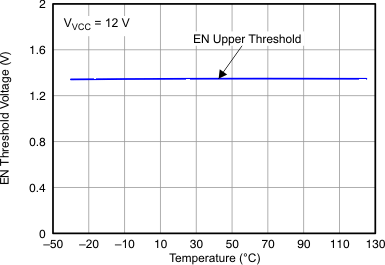
| Upper threshold voltage | 1.30 | 1.35 | 1.40 | V | |
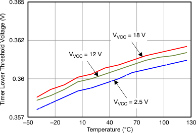
| Lower threshold voltage | 0.33 | 0.35 | 0.37 | V | |
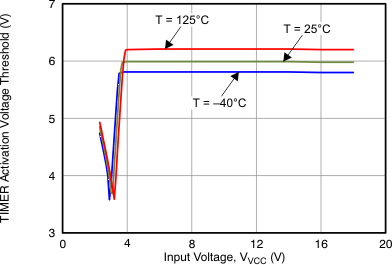
| Timer activation voltage | Raise GATE until ITIMER sinking, measure V(GATE – VCC), VCC = 12 V | 5 | 5.9 | 7 | V |
| Bleed-down resistance | VENSD = 0 V, VTIMER = 2 V | 70 | 104 | 130 | kΩ |
| OUT | |||||
| Input bias current | VOUT = 12 V | 16 | 30 | µA | |
| GATE | |||||
| Output voltage | VOUT = 12 V | 23.5 | 25.8 | 28 | V |
| Clamp voltage | Inject 10 µA into GATE, measure V(GATE – VCC) | 12 | 13.9 | 15.5 | V |
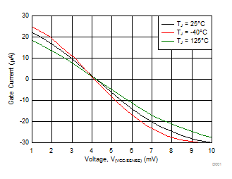
| Sourcing current | VGATE = 12 V | 20 | 30 | 40 | µA |
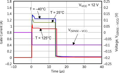
| Sinking current | Fast turnoff, VGATE = 14 V | 0.5 | 1 | 1.4 | A |
| Sustained, VGATE = 4 V to 23 V | 6 | 11 | 20 | mA | |
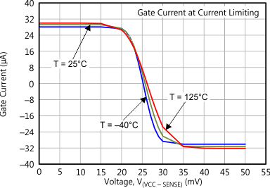
| In inrush current limit, VGATE = 4 V to 23 V | 20 | 30 | 40 | µA | |
| Pulldown resistance | Thermal shutdown | 14 | 20 | 26 | kΩ |
| SENSE | |||||
| Input bias current | VSENSE = 12 V, sinking current | 30 | 40 | µA | |
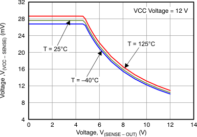
| Current limit threshold | VOUT = 12 V | 22.5 | 25 | 27.5 | mV |
| Power limit threshold | VOUT = 7 V, RPROG = 50 kΩ | 10.1 | 11.6 | 13.1 | mV |
| VOUT = 2 V, RPROG = 25 kΩ | 10.1 | 11.6 | 13.1 | ||
| Fast-trip threshold | 52 | 60 | 68 | mV | |
| OTSD | |||||
| Threshold, rising | 130 | 140 | °C | ||
| Hysteresis(1) | 10 | °C | |||
(1) Parameters are for reference only, and do not constitute part of TI’s published specifications for purposes of TI’s product warranty.
7.6 Timing Requirements
| MIN | NOM | MAX | UNIT | ||
|---|---|---|---|---|---|
| EN | |||||
| Turnoff time | EN ↓ to VGATE < 1 V, CGATE = 33 nF | 20 | 60 | 150 | µs |
| Deglitch time | EN ↑ | 8 | 14 | 18 | µs |
| Disable delay | EN ↓ to GATE ↓, CGATE = 0, tpff50–90, See Figure 1 | 0.1 | 0.4 | 1 | µs |
| PG, PGb | |||||
| Delay (deglitch) time | Rising or falling edge | 2 | 3.4 | 6 | ms |
| GATE | |||||
| Fast-turnoff duration | 8 | 13.5 | 18 | µs | |
| Turn on delay | VCC rising to GATE sourcing, tprr50-50, See Figure 2 | 100 | 250 | µs | |
| SENSE | |||||
| Fast-turnoff duration | 8 | 13.5 | 18 | µs | |
| Fast-turnoff delay(1) | V(VCC – SENSE) = 80 mV, CGATE = 0 pF, tprf50–50, See Figure 3 | 200 | ns | ||
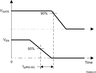 Figure 1. tpff50–90 Timing Definition
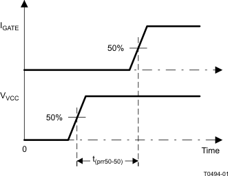 Figure 2. tprr50–50 Timing Definition
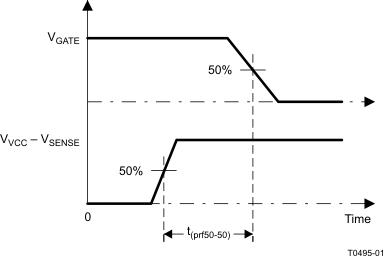 Figure 3. tprf50–50 Timing Definition
7.7 Typical Characteristics
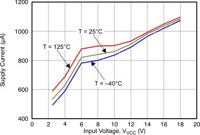
| EN = High |
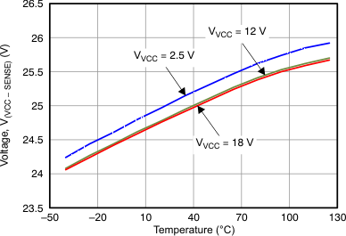
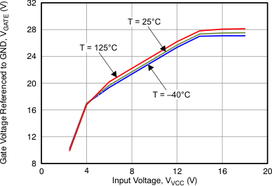
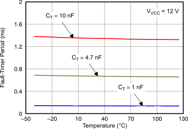
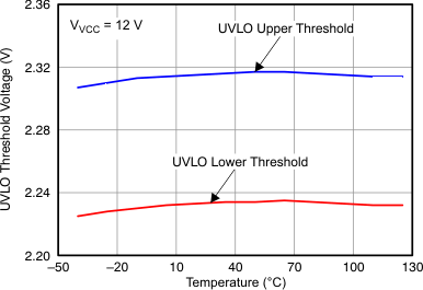
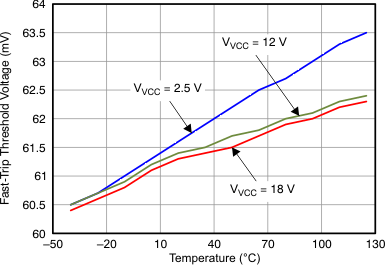

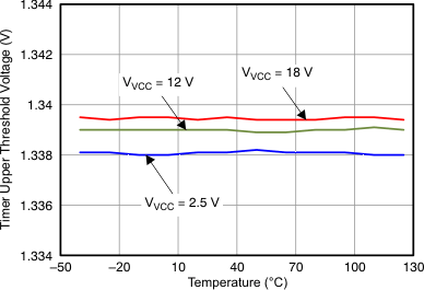
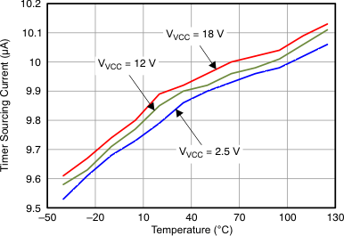
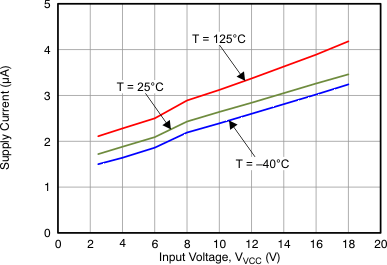
| EN = 0 V |
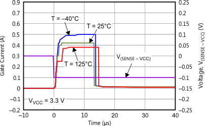
| VVCC = VGATE = 3.3 V | ||
