ZHCSDK8 March 2015 TPS24770 , TPS24771 , TPS24772
PRODUCTION DATA.
- 1 特性
- 2 应用
- 3 说明
- 4 简化电路原理图
- 5 修订历史记录
- 6 Device Comparison Table
- 7 Pin Configuration and Functions
- 8 Specifications
-
9 Detailed Description
- 9.1 Overview
- 9.2 Functional Block Diagram
- 9.3
Feature Description
- 9.3.1 Enable and Over-voltage Protection
- 9.3.2 Current Limit and Power Limit during Start-up
- 9.3.3 Two Level Protection During Regular Operation
- 9.3.4 Dual Timer (TFLT and TINR)
- 9.3.5 3 Options for Response to a Fast Trip
- 9.3.6 Using Soft Start - IHGATE and TINR Considerations
- 9.3.7 Analog Current Monitor
- 9.3.8 Power Good Flag
- 9.3.9 Fault Reporting
- 9.4 Device Functional Modes
-
10Application and Implementation
- 10.1 Application Information
- 10.2
Typical Application
- 10.2.1 12 V, 100 A, 5,500 µF Analog Hot Swap Design
- 10.2.2 Design Requirements
- 10.2.3
Detailed Design Procedure
- 10.2.3.1 Select RSNS and VSNS,CL Setting
- 10.2.3.2 Selecting the Fast Trip Threshold and Filtering
- 10.2.3.3 Selecting the Hot Swap FET(s)
- 10.2.3.4 Select Power Limit
- 10.2.3.5 Set Fault Timer
- 10.2.3.6 Check MOSFET SOA
- 10.2.3.7 Choose Under Voltage and Over Voltage Settings
- 10.2.3.8 Selecting C1 and COUT
- 10.2.3.9 Adding CENHS
- 10.2.3.10 Selecting D1 and D2
- 10.2.3.11 Checking Stability
- 10.2.3.12 Compute Tolerances
- 10.2.4 Application Curves
- 10.2.5
240 VA Application Using CSD16415Q5B
- 10.2.5.1 Design Requirements
- 10.2.5.2 Theory of Operations
- 10.2.5.3
Design Procedure
- 10.2.5.3.1
Select VSNS,CL, RSNS, and RSET Setting
- 10.2.5.3.1.1 Select RPOW and RIMON
- 10.2.5.3.1.2 Selecting the Hot Swap FET(s)
- 10.2.5.3.1.3 Keeping MOSFET within SOA During Normal Start-up
- 10.2.5.3.1.4 Choose Fault Timer
- 10.2.5.3.1.5 Choose Under Voltage and Over Voltage Settings
- 10.2.5.3.1.6 Selecting CIN and COUT
- 10.2.5.3.1.7 Selecting D1 and D2
- 10.2.5.3.1.8 Adding CENHS
- 10.2.5.3.1.9 Stability Considerations
- 10.2.5.3.1
Select VSNS,CL, RSNS, and RSET Setting
- 10.2.5.4 Application Curves
- 10.2.6 240 VA Application Using CSD17573Q5B
- 11Power Supply Recommendations
- 12Layout
- 13器件和文档支持
- 14机械、封装和可订购信息
8 Specifications
8.1 Absolute Maximum Ratings
over operating free-air temperature range (unless otherwise noted) (1)| MIN | MAX | UNIT | ||
|---|---|---|---|---|
| Input Voltage | VDD,SET, FSTP,SENM, OUTH, ENHS, FLTb, PGHS, OV | –0.3 | 30 | V |
| HGATE to OUTH | –0.3 | 15 | V | |
| SET to VDD | –0.3 | 0.3 | V | |
| SENM, FSTP to VDD | –0.6 | 0.3 | V | |
| TINR, TFLT, PLIM, IMON | –0.3 | 3.6 | V | |
| IMONBUF | –0.3 | 7 | V | |
| Sink Current | FLTb, PGHS | 5 | mA | |
| Source Current | IMON, IMONBUF | 5 | mA | |
| Storage temperature, Tstg | –65 | 150 | °C | |
(1) Stresses beyond those listed under Absolute Maximum Ratings may cause permanent damage to the device. These are stress ratings only, which do not imply functional operation of the device at these or any other conditions beyond those indicated under Recommended Operating Conditions. Exposure to absolute-maximum-rated conditions for extended periods may affect device reliability.
8.2 ESD Ratings
| VALUE | UNIT | |||
|---|---|---|---|---|
| V(ESD)(1) | Electrostatic discharge | Human-body model (HBM), per ANSI/ESDA/JEDEC JS-001(2) | ±1500 | V |
| Charged-device model (CDM), per JEDEC specification JESD22-C101(3) | ±500 | |||
(1) Electrostatic discharge (ESD) measures device sensitivity and immunity to damage caused by assembly line electrostatic discharges into the device.
(2) JEDEC document JEP155 states that 500-V HBM allows safe manufacturing with a standard ESD control process.
(3) JEDEC document JEP157 states that 250-V CDM allows safe manufacturing with a standard ESD control process.
8.3 Recommended Operating Conditions
over operating free-air temperature range (unless otherwise noted)| MIN | MAX | UNIT | ||
|---|---|---|---|---|
| Input voltage | VDD, SENM, SET, FSTP | 2.5 | 18 | V |
| ENHS, FLTb, PGHS, OUTH | 0 | 18 | ||
| Sink current | FLTb, PGHS | 0 | 2 | mA |
| Source current | IMON | 0 | 1 | mA |
| External resistance | PLIM | 4.99 | 500 | kΩ |
| IMON | 1 | 6 | kΩ | |
| FSTP | 10 | 4000 | Ω | |
| SET | 10 | 400 | Ω | |
| RIMON / RSET | w/o RSTBL | 10 | 70 | |
| With appropriate RSTBL(1) | 3 | 10 | ||
| with CHGATE > 47nF (2) | 10 | 200 | ||
| External capacitor | TINR, TFLT | 1 | nF | |
| HGATE, (2) | 0 | 1 | µF | |
| IMON | 30 | pF | ||
| IMONBUF | 100 | pF | ||
| Operating junction temperature, TJ | –40 | 125 | °C | |
(1) Refer to RSTBL Requirment for RIMON / RSET < 10 as described in section Select RSNS and VSNS,CL Setting.
(2) External capacitance tied to HGATE, should be in series with a resistor no less than 1kΩ.
8.4 Thermal Information
| THERMAL METRIC(1) | RGE | UNIT | |
|---|---|---|---|
| 24 PINS | |||
| RθJA | Junction-to-ambient thermal resistance | 34.6 | °C/W |
| RθJC(top) | Junction-to-case (top) thermal resistance | 38.4 | |
| RθJB | Junction-to-board thermal resistance | 12.9 | |
| ψJT | Junction-to-top characterization parameter | 0.5 | |
| ψJB | Junction-to-board characterization parameter | 12.9 | |
| RθJC(bot) | Junction-to-case (bottom) thermal resistance | 3.2 | |
(1) For more information about traditional and new thermal metrics, see the IC Package Thermal Metrics application report, SPRA953.
8.5 Electrical Characteristics
Unless otherwise noted these limits apply to the following: -40°C < TJ<125°C; 2.5V < VVDD, VOUT < 18V; VENHS = 2 V; VOV = 0 V; VHGATE, VPGHS, VFLTB, and VIMONBUF are floating; CINR = 1nF; CFLT = 1nF; RSET = 44.2 Ω; RIMON = 2.98k Ω; RFSTP = 200 Ω; RPLIM = 52 kΩ.| PARAMETER | TEST CONDITION | MIN | TYP | MAX | UNIT | |
|---|---|---|---|---|---|---|
| INPUT SUPPLY (VDD) | ||||||
| VUVR | UVLO threshold, rising | 2.2 | 2.32 | 2.45 | V | |
| VUVhyst | UVLO hysteresis | 0.10 | V | |||
| IQON | Supply current: IVDD + IOUTH | Device on, VENHS = 2V | 2.95 | 4 | mA | |
| Hot Swap FET ENABLE (ENHS) | ||||||
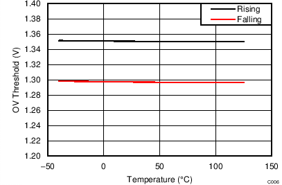
| VENHS | Threshold voltage, rising | 1.3 | 1.35 | 1.4 | V | |
| VENHShyst | Hysteresis | 50 | mV | |||
| IENHS | Input Leakage Current | 0 ≤ VENHS ≤ 30V | –1 | 1 | µA | |
| OVER VOLTAGE (OV) | ||||||
| VOVR | Threshold voltage, rising | 1.3 | 1.35 | 1.4 | mV | |
| VOVhyst | Hysteresis | 50 | mV | |||
| IOV | Input leakage current | 0 ≤ VOV ≤ 30V | –1 | 1 | µA | |
| POWER LIMIT PROGRAMING (PLIM) | ||||||
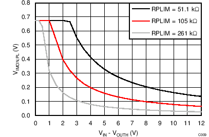
| VPLIM,BIAS | Bias voltage | Sourcing 10μA | 0.65 | 0.675 | 0.7 | V |
| VIMON,PL | Regulated IMON voltage during power limit | RPLIM = 52 kΩ; VSENM-OUTH=12V | 114.75 | 135 | 155.25 | mV |
| RPLIM = 105 kΩ; VSENM-OUTH=12V | 56.95 | 67 | 77.05 | |||
| RPLIM = 261 kΩ; VSENM-OUTH=12V | 18.9 | 27 | 35.1 | |||
| RPLIM = 105 kΩ; VSENM-OUTH=2V | 341.7 | 402 | 462.3 | |||
| RPLIM = 105 kΩ; VSENM-OUTH=18V | 38.25 | 45 | 51.75 | |||
| SLOW TRIP THRESHOLD (SET) | ||||||
| VOS_SET | Input referred offset (VSNS to VIMON scaling) | RSET = 44.2Ω; RIMON=3kΩ to 1.2kΩ (VSNS,CL=10mV to 25mV) | –150 | 150 | µV | |
| VGE_SET | Gain error (VSNS to VIMON scaling)(1) | –0.4% | 0.4% | |||
| FAST TRIP THRESHOLD PROGRAMMING (FSTP) | ||||||
| IFSTP | FSTP input bias current | VFSTP=12V | 95 | 100 | 105 | µA |
| VFASTRIP | Fast trip threshold | RFSTP = 200 Ω, VSNS when VHGATE ↓ | 18 | 20 | 22 | mV |
| RFSTP = 1 kΩ, VSNS when VHGATE ↓ | 95 | 100 | 105 | |||
| RFSTP = 4 kΩ, VSNS when VHGATE ↓ | 380 | 400 | 420 | |||
| CURRENT SUMMING NODE (IMON) | ||||||
| VIMON,CL | Slow trip threshold at summing node | VIMON↑, when ITFLT starts sourcing | 660 | 675 | 690 | mV |
| IIMON-LKG | IMON leakage current | VENHS =0V, VIMON = 1.5V | –200 | 200 | nA | |
| CURRENT MONITOR (IMONBUF) | ||||||
| VOS_IMONBUF | Buffer offset | VIMON = 50mV to 675mV, Input referred | –3 | 0 | 3 | mV |
| GAINIMONBUF | Buffer voltage gain | ΔVIMONBUF / ΔVIMON | 2.97 | 2.99 | 3.01 | V |
| BWIMONBUF | Buffer closed loop bandwidth | CIMONBUF = 75pF | 1 | MHz | ||
| Hot Swap GATE DRIVER (HGATE) | ||||||
| VHGATE | HGATE output voltage | 5 ≤ VVDD ≤ 16V; measure VHGATE-OUTH | 12 | 13.6 | 15.5 | V |
| 2.5V <VVDD < 5V; 16V <VVDD < 20V measure VHGATE-OUTH |
7 | 7.95 | 15 | V | ||
| VHGATEmax | Clamp voltage | Inject 10μA into HGATE, measure V(HGATE – OUTH) | 12 | 13.9 | 15.5 | V |
| IHGATEsrc | Sourcing current | VHGAT-OUTH = 2V-10V | 44 | 55 | 66 | µA |
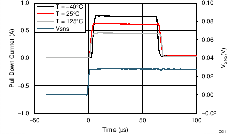
| IHGATEfastSink | Sinking current for fast trip | VHGATE-OUTH = 2V–15V; V(FSTP – SENM) = 20mV | 0.45 | 1 | 1.6 | A |
| IHGATEsustSink | Sustained sinking current | Sustained, VHGATE-OUTH = 2V – 15V; VENHS = 0 | 30 | 44 | 60 | mA |
| INRUSH TIMER (TINR) | ||||||
| ITINRsrc | Sourcing current | VTINR = 0V, In power limit or current limit | 8 | 10.25 | 12.5 | µA |
| ITINRsink | Sinking current | VTINR = 2V, In regular operation | 1.5 | 2 | 2.5 | µA |
| VTINRup | Upper threshold voltage | Raise VTINR until HGATE starts sinking | 1.3 | 1.35 | 1.4 | V |
| VTINRlr | Lower threshold voltage | Raise VTINR to 2V. Reduce VTINR until ITINR is sourcing. | 0.33 | 0.35 | 0.37 | v |
| RTINR | Bleed down resistance | VVDD = 0V, VTINR = 2V | 70 | 104 | 130 | kΩ |
| ITINR-PD | Pulldown current | VTINR = 2V, when VENHS = 0V | 2 | 4.2 | 7 | mA |
| RETRYCYCLE | Cycle number | # of timer cycles before retry (TPS24771 only) | 64 | 64 | 64 | |
| RETRYDUTY | Retry duty cycle | TFLT and TINR connected (TPS24771 only) | 0.70% | |||
| TFLT and TINR not connected (TPS24771 only) | 0.35% | |||||
| VIMON,TINR | See Using Soft Start - IHGATE and TINR Considerations | RPLIM = 52kΩ, VSENM = 12V, VOUTH = 0 V. Raise IMON voltage and record IMON when TINR starts sourcing current. | 47.75 | 90 | 132.25 | mV |
| VIMON,PL | See Using Soft Start - IHGATE and TINR Considerations | RPLIM = 52kΩ, VSENM-OUTH = 12V, Raise IMON voltage and record IMON when IHGATE starts sinking current. | 114.75 | 135 | 155.25 | mV |
| ΔVIMON,TINR | See Using Soft Start - IHGATE and TINR Considerations | ΔVIMON,TINR = VIMON,PL - VIMON,TINR | 23 | 45 | 67 | mV |
| FAULT TIMER (TFLT) | ||||||
| ITFLTsrc | Sourcing current | VTFLT = 0V, PGHS is high and in overcurrent | 8 | 10.25 | 12.5 | µA |
| ITFLTsink | Sinking current | VTFLT = 2V, Not in overcurrent | 1.5 | 2 | 2.5 | µA |
| VTFLTup | Upper threshold voltage | Raise VTFLT until HGATE starts sinking | 1.3 | 1.35 | 1.4 | V |
| RTFLT | Bleed down resistance | VENHS = 0V, VTFLT = 2V | 70 | 104 | 130 | kΩ |
| ITFLT-PD | Pulldown current | VTFLT = 2V, when VENHS = 0V | 2 | 5.6 | 7 | mA |
| HOT SWAP OUTPUT (OUTH) | ||||||
| IOUTH, BIAS | Input bias current | VOUTH = 12V | 30 | 70 | µA | |
| FAULT INDICATOR (FLTb) | ||||||
| VOL_FLTb | Output low voltage | Sinking 2 mA | 0.11 | 0.25 | V | |
| IFLTb | Input leakage current | VFLTb = 0V, 30V | –1 | 0 | 1 | µA |
| VHSFLT_IMON | VIMON threshold to detect Hot Swap FET short | VENHS = 0V, Measured VIMON ↑ to GND when FLTb ↓ | 88 | 101 | 115 | mV |
| VHSFL_hyst | Hysteresis | 25 | mV | |||
| HOT SWAP POWER GOOD OUTPUT (PGHS) | ||||||
| VPGHSth | PGHS Threshold | Measure VSENM-OUTH ↓ when PGHS↑ | 170 | 270 | 375 | mV |
| VPGHShyst | PGHS hysteresis | VSENM-OUTH ↑ | 80 | mV | ||
| VOL_PGHS | PGHS Output low voltage | Sinking 2mA | 0.11 | 0.25 | V | |
| IPGHS | PHGS Input leakage current | VPGHS=0V to 30V | –1 | 0 | 1 | µA |
| THERMAL SHUTDOWN (OTSD) | ||||||
| TOTSD | Thermal shutdown threshold | Temperature rising | 140 | °C | ||
| TOTSD,HYST | Hysteresis | 10 | °C | |||
(1) Specified by characterization.
8.6 Timing Requirements
| PARAMETER | TEST CONDITION | MIN | TYP | MAX | UNIT | |
|---|---|---|---|---|---|---|
| INPUT SUPPLY (VDD) | ||||||
| DEGLUVLO | UVLO deglitch | Both rising and falling | 14 | µs | ||
| HOT SWAP FET ENABLE (ENHS) | ||||||
| DEGLENHS | Deglitch time | Both rising and falling | 2.2 | 3.8 | 5.5 | µs |
| OVER VOLTAGE (OV) | ||||||
| DEGLOV | Deglitch time | Both rising and falling | 2.2 | 3.9 | 5.7 | µs |
| FAST TRIP (FSTP) | ||||||
| tFastOffDly | Fast turn-off delay | V(FSTP – SENM) : –5mV to 5mV, CHGATE = 0 pF | 600 | ns | ||
| V(FSTP – SENM) : -20mV to 20mV CHGATE = 0 pF | 300 | |||||
| tFastOffDur | Strong pull down current duration | 53 | 63 | 73 | µs | |
| INRUSH TIMER (TINR) | ||||||
| NRETRY | Number of TINR cycles before retry | TPS24741 only | 64 | |||
| RETRYDUTY | Retry duty cycle | TINR not connected to TFLT | 0.35% | |||
| TINR connected to TFLT | 0.7% | |||||
| FAULT INDICATOR (FLTb) | ||||||
| tFLT_degl | Fault deglitch | Both rising and falling | 2.2 | 3.9 | 5.3 | ms |
| HOT SWAP POWER GOOD OUTPUT (PGHS) | ||||||
| tPGHSdegl | PGHS deglitch time | Rising | 0.7 | 1 | 1.3 | ms |
| Falling | 7 | 8 | 9 | |||
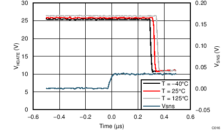
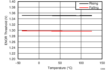
8.7 Typical Characteristics
Unless otherwise noted these cureves apply to the following: -40°C < TJ<125°C; 2.5V < VVDD, VOUT < 18V; VENHS = 2 V; VOV = 0 v; VHGATE, VPGHS, VFLTB, and VIMONBUF are floating; CINR = 1nF; CFLT = 1nF; RSET = 44.2 Ω; RIMON = 2.98k Ω; RFSTP = 200 Ω; RPLIM = 52 kΩ.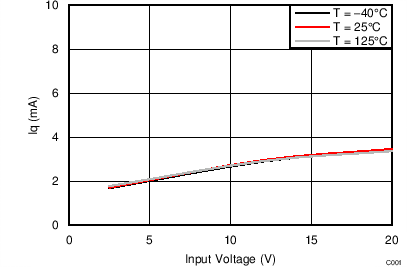
| Iq = IVDD+IOUTH |
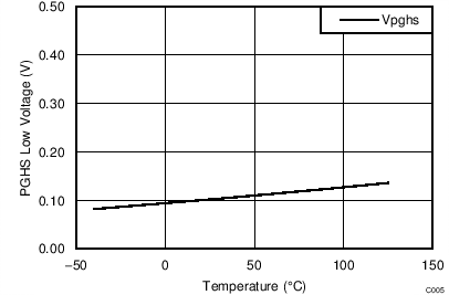
| IPGHS =2mA |
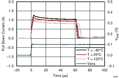
| VHGATE-VOUTH=10V |
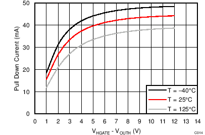
| Sustained sink current | ||
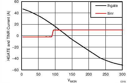
| VHGATE-OUTH=4V | ||
| RPLIM =52kΩ | ||
| TJ =25°C |
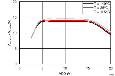
| VIMON during Power Limiting | ||
| VHGATE-VOUTH=2V |
