ZHCSDK8 March 2015 TPS24770 , TPS24771 , TPS24772
PRODUCTION DATA.
- 1 特性
- 2 应用
- 3 说明
- 4 简化电路原理图
- 5 修订历史记录
- 6 Device Comparison Table
- 7 Pin Configuration and Functions
- 8 Specifications
-
9 Detailed Description
- 9.1 Overview
- 9.2 Functional Block Diagram
- 9.3
Feature Description
- 9.3.1 Enable and Over-voltage Protection
- 9.3.2 Current Limit and Power Limit during Start-up
- 9.3.3 Two Level Protection During Regular Operation
- 9.3.4 Dual Timer (TFLT and TINR)
- 9.3.5 3 Options for Response to a Fast Trip
- 9.3.6 Using Soft Start - IHGATE and TINR Considerations
- 9.3.7 Analog Current Monitor
- 9.3.8 Power Good Flag
- 9.3.9 Fault Reporting
- 9.4 Device Functional Modes
-
10Application and Implementation
- 10.1 Application Information
- 10.2
Typical Application
- 10.2.1 12 V, 100 A, 5,500 µF Analog Hot Swap Design
- 10.2.2 Design Requirements
- 10.2.3
Detailed Design Procedure
- 10.2.3.1 Select RSNS and VSNS,CL Setting
- 10.2.3.2 Selecting the Fast Trip Threshold and Filtering
- 10.2.3.3 Selecting the Hot Swap FET(s)
- 10.2.3.4 Select Power Limit
- 10.2.3.5 Set Fault Timer
- 10.2.3.6 Check MOSFET SOA
- 10.2.3.7 Choose Under Voltage and Over Voltage Settings
- 10.2.3.8 Selecting C1 and COUT
- 10.2.3.9 Adding CENHS
- 10.2.3.10 Selecting D1 and D2
- 10.2.3.11 Checking Stability
- 10.2.3.12 Compute Tolerances
- 10.2.4 Application Curves
- 10.2.5
240 VA Application Using CSD16415Q5B
- 10.2.5.1 Design Requirements
- 10.2.5.2 Theory of Operations
- 10.2.5.3
Design Procedure
- 10.2.5.3.1
Select VSNS,CL, RSNS, and RSET Setting
- 10.2.5.3.1.1 Select RPOW and RIMON
- 10.2.5.3.1.2 Selecting the Hot Swap FET(s)
- 10.2.5.3.1.3 Keeping MOSFET within SOA During Normal Start-up
- 10.2.5.3.1.4 Choose Fault Timer
- 10.2.5.3.1.5 Choose Under Voltage and Over Voltage Settings
- 10.2.5.3.1.6 Selecting CIN and COUT
- 10.2.5.3.1.7 Selecting D1 and D2
- 10.2.5.3.1.8 Adding CENHS
- 10.2.5.3.1.9 Stability Considerations
- 10.2.5.3.1
Select VSNS,CL, RSNS, and RSET Setting
- 10.2.5.4 Application Curves
- 10.2.6 240 VA Application Using CSD17573Q5B
- 11Power Supply Recommendations
- 12Layout
- 13器件和文档支持
- 14机械、封装和可订购信息
9 Detailed Description
9.1 Overview
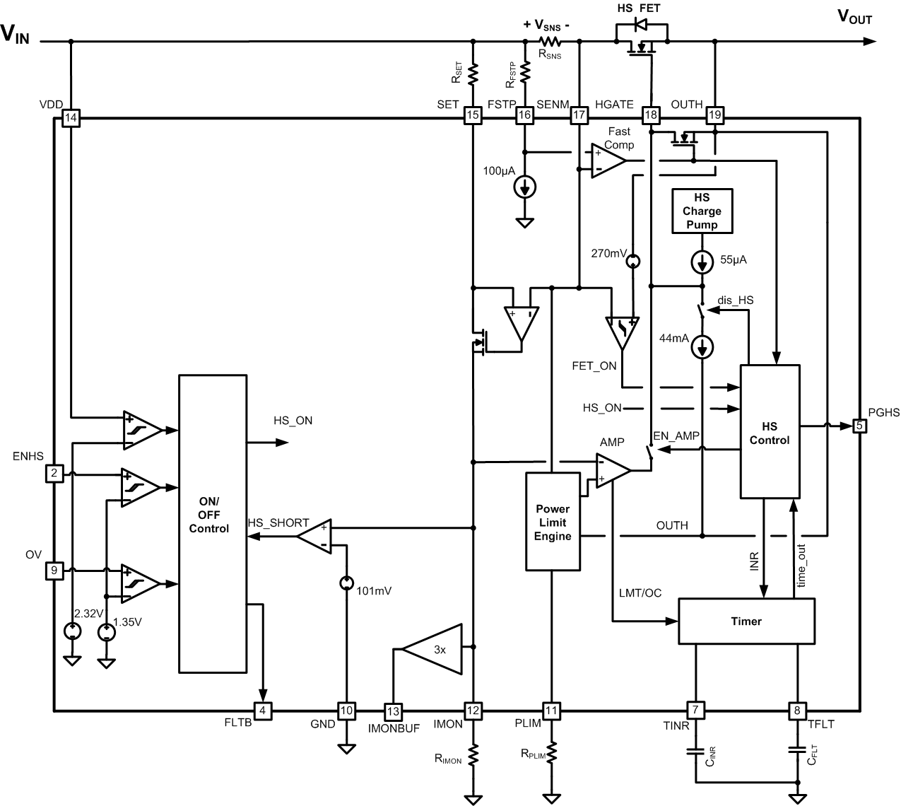
The TPS2477x Hot Swap features a programmable current limit, power limit, and fast trip threshold. It also has dual timers: one for inrush and one during over current faults. Finally it features an analog current monitor that can be used to provide current information to a microcontroller.
9.2 Functional Block Diagram
9.3 Feature Description
9.3.1 Enable and Over-voltage Protection
The part is enabled when the ENHS pin voltage exceeds 1.35V and is disabled when the pin voltage falls under 1.3V providing 50mV of hysteresis. A resistor divider can be connected to these pins to turn on the TPS2477x at a certain bus voltage. The part will turn off if the OV pin exceeds 1.35V.
9.3.2 Current Limit and Power Limit during Start-up
The current limit and power limit of the TPS2477x are programmable to protect the load, power supply, and the Hot Swap MOSFET. During start-up the active control loop will regulate the gate to ensure that the current through the MOSFET and the power dissipation of the MOSFET is below their respective pre-programmed thresholds. The maximum current allowed through the MOSFET (ILIM) is determined with the equation below. ILIM,CL is the programmed current limit, PLIM is the programmed power limit, and VDS is the drain to source voltage across the Hot Swap MOSFET.

This results in an IV curve shown in Figure 12. ILIM,PL denotes the maximum allowed MOSFET current (IDS) when the part is in power limit. As VDS increases, ILIM,PL decreases and ILIM,PL,MIN denotes the lowest ILIM,PL, which occurs at the largest VDS (VDS,MAX). The TPS2477x enforce this by regulating the voltage across RSNS (VSNS). VSNS,PL denotes VSNS when power limiting is active. Similarly to ILIM,PL, VSNS,PL decreases as VDS increases and VSNS,PL,MIN corresponds to the lowest VSNS,PL, which occurs at VDS,MAX. VSNS,CL is a current limiting sense voltage, which is programmable in the TPS2477x.
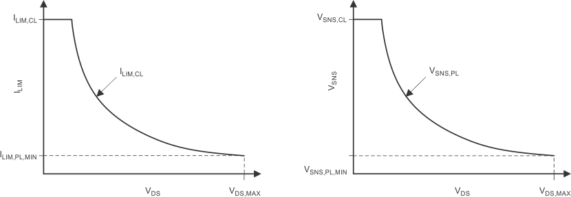 Figure 12. Current vs VDS and VSNS vs VDS Programmed by Power Limit Engine.
The current and power limit can be programmed using the equations below.
sp

sp

sp

Note, that the error is largest at VSNS,PL,MIN due to offset of the internal amplifier. Also the operation at VDS,MAX is most critical because it corresponds to the short circuit condition and has the biggest impact on start time. Thus it is critical to consider VSNS,PL,MIN during design. Equation 5 shows the relationship of VSNS,PL,MIN as a function of PLIM, ILIM,CL, VSNS,CL, and VDS,MAX. Note that ILIM,CL and VDS,MAX are usually determined by the system requirements. The designer will have control over PLIM and VSNS,CL. In general, there will be a desire to reduce the power limit to allow for smaller MOSFETs and to reduce the VSNS,CL to improve efficiency (lower RSNS). However, this will also reduce VSNS,PL,MIN and the designer should ensure that it’s above the minimum recommended value of 1.5mV.
sp

9.3.3 Two Level Protection During Regular Operation
After the TPS2477x has gone through start-up it will no longer actively control the gate. Instead it will run the timer when the current is between the current limit and the fast trip threshold. Once the timer has expired the gate will be pulled down. If the current ever exceeds the fast trip threshold, the gate will be pulled down immediately.
9.3.4 Dual Timer (TFLT and TINR)
TPS2477x has two timer pins to allow the user to customize the protection. The TINR pin will source 10.25 µA when the device is in start-up mode and is actively regulating the gate to limit the MOSFET power or current. It will sink 2 µA otherwise. The TFLT pin will source 10.25 µA when the device is in regular operation and the FET current exceeds the current limit. It will sink 2 µA otherwise. If either of the timer pins exceeds 1.35, the TPS2477x will time out. The TPS24770 and TPS24772 will latch off. The TPS24771 will go through 64 cycles of TINR and attempt to start-up again.
Since the TINR usually runs when the MOSFET is being stressed, TINR should be sized to maintain the FET within its SOA. In general TFLT runs when the load is drawing more current than expected, which can stress the load and the power supply. Thus TFLT should be programmed to have the right protection settings for the power supply and the load. In some systems the load is allowed to draw current above the current limit for 250ms or 1s. In that case a large TFLT is required, but a short TINR may still be desired to minimize the worst case FET stress. In other applications a long TINR may be required to due to large downstream capacitances, but drawing excessive current from the power supply for more than 5ms is not desired. In that case a short TFLT and a long TINR should be used. Finally, many applications can use the same TINR and TFLT setting, in which case the pins can be tied together and a single capacitor can be used. The two different options are shown in Figure 13.
 Figure 13. Timer Configurations
If two separate timer capacitors are used their values can be computed with the equations below:
sp

sp

sp
If a single capacitor is used CTMR can be computed with Equation 8.

9.3.5 3 Options for Response to a Fast Trip
The TPS24770, TPS24771, and TPS24772 have difference responses to a fast trip event to accommodate different design requirements. When the current exceeds the fast trip threshold, the gate is quickly pulled down to minimize damage that can be caused due to a short circuit. Figure 14 shows the response of the variout devices options to a hot short on the output. The TPS24770 (latch) will attempt to re-start once after the hot-short is observed and then stay off, the TPS24771 will continuously retry with a duty cycle of ~0.5% (0.7% if TFLT and TINR are connected, 0.35% if TFLT and TINR are not connected), and the TPS24772 (fast latch off) will shut off and never retry again. In general the TPS24772 will place the least amount of stress on the MOSFET, but is the least likely to recover from a nuissance trip.
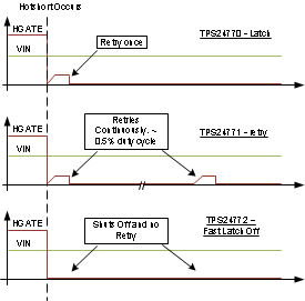 Figure 14. TPS24770/1/2 Response to a Short Circuit
9.3.6 Using Soft Start - IHGATE and TINR Considerations
During start-up the TPS2477x regulates the HGATE to keep the FET power dissipation within PLIM. This is accomplished by an amplifier that monitors the IMON voltage and an internal reference voltage. The TPS2477x will source current into HGATE if VIMON is lower than the reference voltage and will sink current into HGATE if VIMON is above the reference voltage. In steady state, the VIMON will be regulated to the VIMON,PL point, where IHGATE equals zero. Note that VIMON,PL is a determined by RPLIM and VSENM – VOUTH.
The same amplifier feeds into the inrush timer circuitry to run the timer when the part is in power limit. The VIMON threshold at which the timer starts to source current is denoted as VIMON, TINR. Note that VIMON,TINR is lower than VIMON,PL to account for tolerances and ensure that the timer is always active when the device is in power limit. The difference between the two thresholds is defined as ΔVIMON, TINR. Refer to Figure 11 for a typical IHGATE and ITINR vs VIMON curve.
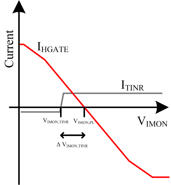 Figure 15. ITINR and IHGATE vs VIMON (VDS = 12V, RPLIM = 52kΩ)
It is critical to consider ΔVIMON, TINR and Figure 15 if a soft start circuit is used. Typically, the soft start is implemented by limiting the gate dv/dt with a capacitor, which in turn limits the inrush current to the output capacitor. Often times, the inrush current is kept below ILIM,PL to keep the timer from running. Note that the ILIM,PL is based on the VIMON,PL threshold and thus TINR can be activated even if the inrush current is below ILIM,PL. To prevent the timer from running unintentionally, the PLIM should be chosen above PLIM,MIN,SS, which can be computed as shown below. As an example consider the usage case where the maximum inrush current (IINR,MAX) is 2A, the maximum input voltage (VIN,MAX) is 13V and RSET, RIMON, and RSNS are 100Ω, 2.7kΩ, and 1mΩ respectively. For that case the power limit should be set to at least 58.3 W + PLIM tolerance to ensure that the inrush timer doesn’t run.

9.3.7 Analog Current Monitor
The TPS2477x also features two analog current monitoring outputs: IMON and IMONBUF. Each has their own advantages and disadvantages. The IMON is more accurate, because it doesn’t have the error added from the second stage. However it is a high impedance output and leakage current on that node would result in monitoring error. In addition it can only support 30pF of capacitance and its full scale range is 675mV (this is where current limit kicks in). The IMONBUF takes the IMON signal and buffers it 3x. This introduces more error, but the output is low impedance, has a larger full scale range, and can drive up to 100pF of capacitance.
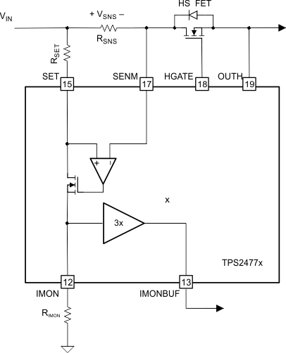 Figure 16. Current Monitoring Circuitry
9.3.8 Power Good Flag
The TPS2477x has a power good flag, which should be used to turn on downstream DC/DC converters. This reduces the stress on the Hot Swap MOSFET during start-up. The PGHS pin of the TPS2477x is asserted (with 1 ms deglitch) when both:
- Hot Swap is enabled and
- VDS of Hot Swap MOSFET is below 240 mV.
PGHS is de-asserted (with 8 ms deglitch) when either:
- Hot Swap is disabled.
- VDS of Hot Swap MOSFET is above 310 mV
- In an overcurrent condition that causes the timer to time out and latch off.
9.3.9 Fault Reporting
TPS2477x will assert a fault by pulling down on the FLTb pin if any of the following occur:
- Hot Swap MOSFET Shorted Fault ( ENHS = LO, but VIMON > 101 mV)
- Hot Swap timer times out.
- Over Temperature Shut Down (OTSD)
9.4 Device Functional Modes
9.4.1 Hot Swap Functional Modes
The state machine for the Hot Swap section is shown in Figure 17. After a POR / UVLO event the Hot Swap enters the Inrush up. Once operational the Hot Swap has the following functional modes:
- Inrush Mode (INR): In this state the Hot Swap controller is actively regulating the HGATE to meet the current limit and power limit settings. The inrush timer is running if the controller is in power or current limiting. If the inrush timer times out the gate will be pulled down. The TPS24770 and TPS24772 will go to latched mode and TPS24771 will go into retry mode.
- Regular Operation Mode (REG): In this mode everything is operating properly so both the timers are discharged and the HGATE is high. If there is an overcurrent condition (VSNS > VSNS,CL), the device will go into fault mode. If there is a fast trip condition (VSNS > VFSTP), the gate will be pulled down with a 1A / 63 µs pulse. The TPS24772 will go to the latched state and the TPS24770 and TPS24771 will go back to inrush for a retry.
- Fault Mode (FLT): In this mode the TPS2477x runs the fault timer. Once the timer expires the TPS24770 and TPS24772 will go to latch mode while TPS24771 will go to retry mode. If the overcurrent condition is removed the controller will go back to the regular operation mode.
- Latched Mode (Latched): In the latched mode the HGATE is low, the timer is being discharged, and the FLTb is asserted. If there is a rising edge on ENHS the part will discharge the timers and go to the inrush mode.
- Retry Mode (Retry): Here the part will charge and discharge the inrush timer 64 times before attempting another retry.
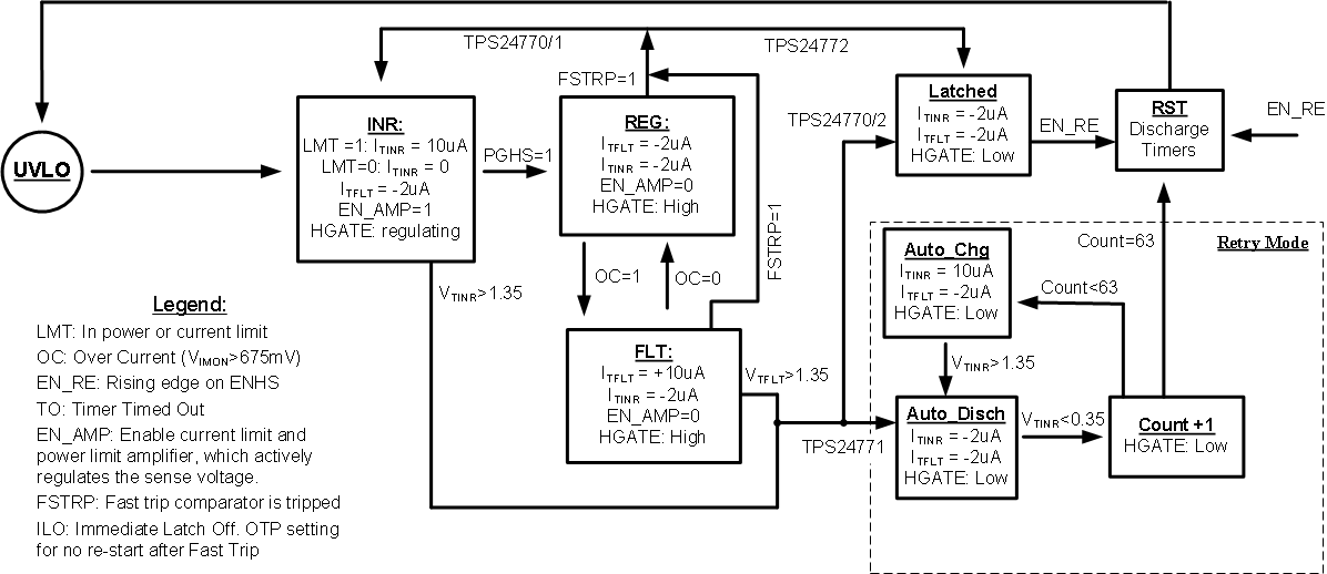 Figure 17. Hot Swap State Machine